PLL stands for Phase Locked Loop. As the name implies and as shown in the illustration below, PLL is a kind of a circuit with feedback LOOP to keep the phase/frequency of feedbacked signal same (LOCKED) as the phase/frequency of Reference Input Signal.
A PLL sits inside almost every radio. It removes jitter from a reference clock, recovers the carrier or the clock of a received signal, and generates the local oscillator of a transmitter or a receiver. All of these jobs use the same loop. So let's first go through the blocks of that loop and the simplest phase detector. Then we'll see why a better phase detector is needed, how a divider turns the loop into a frequency synthesizer, and why a phase detector can lock a frequency at all.
- What are the blocks of a PLL ?
- How does a simple XOR phase detector work ?
- How can a phase detector tell a lead from a lag ?
- How does a PLL become a frequency synthesizer ?
- How PLL can lock to a specific Frequency ?
What are the blocks of a PLL ?
A PLL has three blocks in the forward path and one path back. Let's name each block and the signal it passes on, because the later sections change one block at a time.
As shown in the following diagram, if there is phase difference between Reference Input and Feedbacked Input, "Phase detector + Loop Filter" generate a certain level of voltage to change (control) VCO (Voltage Controlled Oscillator).
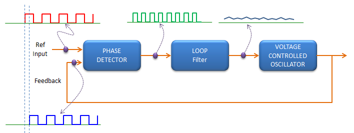
The basic PLL loop. The VCO output is fed back and compared with the reference, and the filtered error steers the VCO.
- The Ref Input, drawn in red, and the Feedback, drawn in blue, both enter the PHASE DETECTOR. The dashed vertical lines at the left mark the small offset between their edges.
- The phase detector output, drawn in green, is a train of short pulses.
- The LOOP Filter output is a nearly flat line with a small ripple on it. This line is the control voltage of the VCO.
- The VOLTAGE CONTROLLED OSCILLATOR output leaves on the right. It also returns along the bottom line and enters the phase detector as the Feedback.
The VCO is the only block that sets the output frequency. Its frequency moves in proportion to the control voltage, fout = f0 + KV x Vctrl. Here f0 is the free running frequency and KV is the VCO gain in Hz per volt. For example, a VCO with f0 = 2.35 GHz and KV = 50 MHz/V runs at 2.4 GHz when the control voltage is 1 V.
The phase detector and the loop filter only decide which control voltage the VCO gets. So the loop is a negative feedback system. If the feedback leads the reference, the control voltage moves the VCO frequency down. If the feedback lags, the VCO frequency moves up. The loop filter also sets how fast the loop reacts. A narrow loop filter removes more ripple from the control voltage, but the loop then needs more time to settle after a change.
The VCO sets the frequency, and the rest of the loop steers it : the phase detector measures the error, and the loop filter turns it into a control voltage.The loop is a negative feedback system : any phase error produces a control voltage that reduces that error.The loop filter trades ripple against speed : a narrower filter gives a cleaner control voltage and a slower loop.
How does a simple XOR phase detector work ?
The phase detector turns a timing difference into a voltage. The simplest one is a single logic gate, so it is a good place to start. After that we'll look at the one thing this gate cannot do.
Now, getting into a little more details.. let's think about how Phase Detector work. There are a couple of different types of phase detector, but in simplest of form of phase detector work as follows. It just compare two signal level of Reference Input signal and feedback signal every points in time domain, if the both signal is ON, Phase detector genete 'OFF' level (Level 0) and if only one of the signal is ON, the phase detector generate 'ON' level. Simply put, in this case the phase detector is exactly same as XOR Gate logic. Therefore, if the phase of the two input signal is different, Phase detector would generate a terain of pulses. The width of pulse is in proportion to the degree of phase difference. Once these pulses are generated, it goes though a Low Pass Filter (it is called LOOP filter) to smoothen out the pulses to make more flat (DC like) signal. And this DC like signal act as control voltage for VCO.
The timing diagram below draws four signals of the loop on one time axis. The dashed vertical lines mark every edge of the Ref Input and the Feedback, so you can check where each pulse starts and ends.
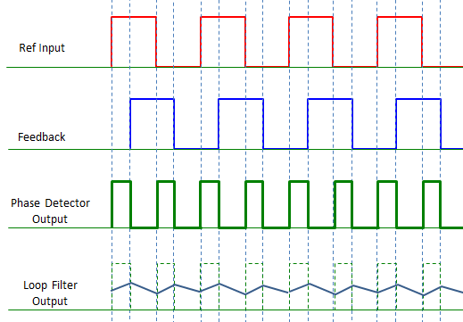
XOR phase detection. A pulse appears wherever the two inputs differ, and the loop filter averages the pulses into a slowly varying voltage.
- Ref Input in red and Feedback in blue are square waves with the same period. The Feedback edges come a little later than the Ref Input edges.
- The Phase Detector Output is high from each red edge to the next blue edge. So there are two pulses in every period.
- The Loop Filter Output rises during each pulse and falls between the pulses. The dashed boxes behind it repeat the pulses to show this.
We can put a number on the pulse width. Let both inputs be square waves with a 50 % duty cycle, and let the phase difference ΔΦ lie between 0 and π radians. Each pulse then lasts ΔΦ/(2π) of a period, and there are two pulses per period. So the duty cycle of the XOR output is ΔΦ/π, and the average voltage after the loop filter is VDD x ΔΦ/π. A phase difference of 90 deg gives half of VDD, and 180 deg gives the full VDD. The slope, VDD/π volts per radian, is the gain of this phase detector.
Looks not so complicated. But there is an issue with the PLL as explained above. If you simply apply the rule explained above, the phase detector cannot make any difference whether the feedback signal phase is leading or lagging in comparison to reference signal phase as illustrated below.
The diagram below repeats the same timing diagram twice. The left panel is titled as a leading feedback, and the right panel as a lagging feedback.
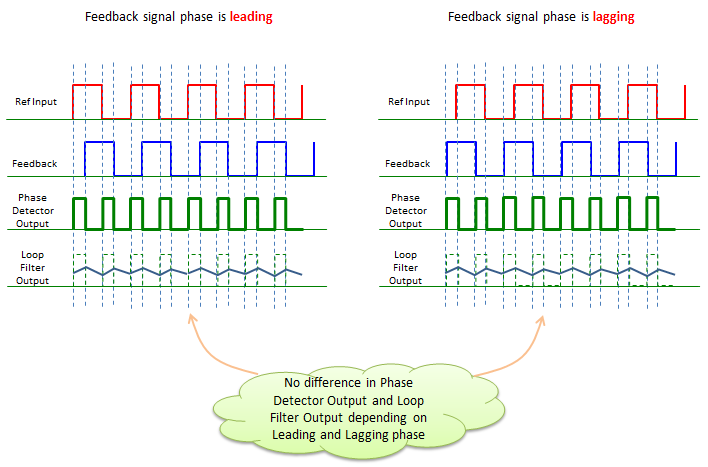
An XOR phase detector cannot tell the sign of the phase error. A lead and a lag of the same size give the same pulse train and the same average voltage.
- Each panel has the same four rows as the diagram above: Ref Input, Feedback, Phase Detector Output and Loop Filter Output.
- The note at the bottom says there is no difference in the phase detector output and the loop filter output between the leading and the lagging phase.
- Measured on the drawing, the blue edges in the left panel come about a fifth of a period after the red edges. In the right panel they come about a sixth of a period before them. So the left panel actually shows a lag and the right panel a lead, the opposite of the two titles. The point of the picture does not change, because the XOR output is the same for both signs.
The formula above shows the reason. The output depends on the size of ΔΦ and not on its sign, because a lead and a lag of the same size produce pulses of the same width. The output also folds back. Between π and 2π the average falls again, as VDD x (2π - ΔΦ)/π. So an XOR loop normally locks near 90 deg, in the middle of one slope. There, a small error in one direction raises the voltage and a small error in the other direction lowers it. This result also assumes both inputs have a 50 % duty cycle. With other duty cycles the XOR output no longer reaches 0 V at zero phase difference.
An XOR gate is the simplest phase detector : its average output is VDD x ΔΦ/π for a phase difference between 0 and 180 deg.The XOR output has no sign : a lead and a lag of the same size give the same voltage.An XOR loop locks near 90 deg, not at 0 deg : only on a slope does the output move in opposite directions for a lead and a lag.
How can a phase detector tell a lead from a lag ?
The XOR detector gives the loop the size of the error but not its direction. A detector with a signed output tells the VCO which way to move straight away, and it lets the loop lock at zero phase difference.
So the next step evolution to PLL would be to develop a phase detector that gives the different result depending on whether the feedback signal phase is leading or lagging in comparison to reference signal phase. In this figure, you see that the phase detector generate output signal with different polarity (different sign) depending on whether the phase is leading or lagging.
Is there any of PLL which is using this kind of detector ? Of course, there are many of these PLL. (I will explain more about the phase detector of this type later when I have time.)
The diagram below uses the same layout as the XOR diagrams above. This time the Phase Detector Output sits above its baseline in the left panel and below its baseline in the right panel.
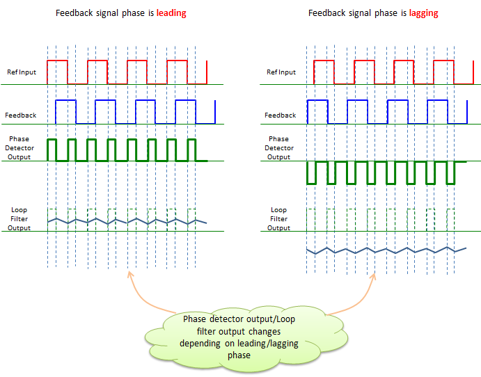
A signed phase detector. The polarity of the output follows the sign of the phase error, so the loop filter output moves up in one case and down in the other.
- In the left panel, titled leading, the Phase Detector Output pulses go up from the baseline. The Loop Filter Output stays near its own line.
- In the right panel, titled lagging, the pulses go down from the baseline. The Loop Filter Output drops well below its line.
- The Ref Input and Feedback rows are drawn with the same edge positions as in the XOR diagram above.
- The note at the bottom says the phase detector output and the loop filter output change depending on leading or lagging phase.
Most synthesizers today use a phase frequency detector, PFD, for this job. A PFD is built from two flip-flops and a reset gate. The reference edge sets an UP output, and the feedback edge sets a DOWN output. When both outputs are set, the gate resets them. So the width of the UP or DOWN pulse equals the time between the two edges, and the name of the pulse gives the sign.
A charge pump usually follows the PFD. It turns an UP pulse into a current into the loop filter and a DOWN pulse into a current out of it. The PFD is linear over a range of +/-2π, while the XOR detector covers a range only π wide. The PFD also keeps giving the right sign when the two frequencies differ. For this reason a PFD pulls a loop into lock from a large frequency error, where an XOR loop can fail.
A signed output lets the loop lock at zero phase error : the polarity tells the VCO whether to move up or down.A PFD with a charge pump is the common signed detector : the width of the UP or DOWN pulse equals the time between the reference edge and the feedback edge.A PFD also detects a frequency error : its output keeps the correct sign when the two frequencies differ, and this helps the loop pull in.
How does a PLL become a frequency synthesizer ?
So far the loop only copies the reference. But a radio needs many output frequencies from one fixed reference crystal. One extra block in the feedback path solves this, and it also brings a cost in phase noise.
Now I think I understand how PLL can detect phase difference and compensate those phase difference. But when I heard that one of the most common application of PLL is frequency synthesize and it implies that it can detect Frequency difference and can lock the output frequency to a specific value. I took me long time to finally understand the correlation between PLL operation and frequency synthesis. The secrete is to put a frequency devider in feedback path as shown below. In this way, we can lock the output frequency of VCO (Voltage Controlled Oscillator) to (N x Ref Input frequency)
The block diagram below is the loop of the first section with one change. A Frequency Divider, marked with a divide sign and N, now sits between the VCO output and the Feedback input.
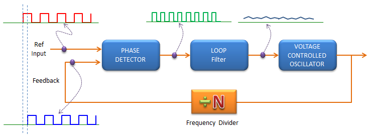
Integer-N synthesizer. The phase detector compares fout/N with the reference, so lock means fout = N x fref.
- The forward path is unchanged: PHASE DETECTOR, LOOP Filter and VOLTAGE CONTROLLED OSCILLATOR.
- The Frequency Divider sits on the bottom line, on the way from the VCO output back to the Feedback input.
- The Ref Input and Feedback waveforms at the left have the same period. The phase detector compares the divider output, not the VCO output, with the reference.
For example, if you put '% 2' divider on the feedback path, you can lock the frequency to twice as high as the frequency of Ref Input frequency.
The diagram below draws this example. The divider is marked with a divide sign and 2, and the red waveform after the VCO has twice as many pulses as the Ref Input waveform.
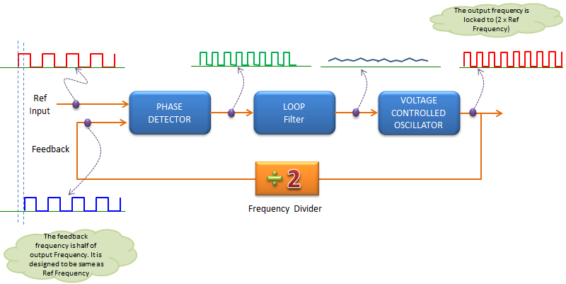
Divide by 2. The loop forces the divided output to match the reference, so the VCO settles at twice the reference frequency.
- The upper note says the output frequency is locked to 2 x Ref Frequency.
- The lower note says the feedback frequency is half of the output frequency, and that it is designed to be the same as the Ref Frequency.
- Over the same time span, the red waveform at the VCO output has twice as many pulses as the Ref Input.
Once N is a variable, the loop becomes a tunable source. The step between two output frequencies equals fref, because N can only change by 1. Take fref = 1 MHz. With N = 2400 the VCO locks to 2400 MHz, and with N = 2401 it locks to 2401 MHz. So a 1 MHz channel raster needs a 1 MHz reference at the phase detector. A finer raster needs a lower fref, and that has a cost. The loop bandwidth has to stay well below fref, so a low fref means a slow loop. Fractional-N synthesizers avoid this limit. They switch N between two neighbouring integers, for example 2400 and 2401, so that the average division ratio is a fraction.
The divider also multiplies the reference noise. Inside the loop bandwidth, the phase noise of the reference and of the phase detector appears at the output raised by 20 log10(N) dB. For N = 2400 this is 67.6 dB. So a synthesizer design keeps N as small as the channel raster allows.
A divider in the feedback path multiplies the frequency : the loop locks when fout/N = fref, so fout = N x fref.An integer-N synthesizer tunes in steps of fref : a finer step needs a lower reference or a fractional-N divider.In-band phase noise grows with N : the reference and phase detector noise rise by 20 log10(N) dB at the output.
How PLL can lock to a specific Frequency ?
The previous sections talk about phase, but a synthesizer promises a frequency. Two short equations connect the two. Once that connection is clear, it is easy to see why a phase detector can lock a frequency.
As you might have noticed, the critial part of PLL mechanism is to detect Phase difference between a reference signal and input signal. But when we talk about PLL, in most case it would refer to a device that can lock a frequecny of a signal to a specific reference frequency. Then, my question was how the Phase detection mechanism can detect the frequency difference. I found it not easy to visualize the relationship between Phase and frequency, but from following mathmatical equations it can be seen obvious that there is a certain deterministic relationship between phase and frequency.
Following equation shows that Phase accumulated over a certain time span is the result of integration of frequency over the same time period.
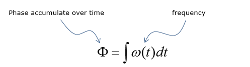
Phase is the running integral of frequency. A frequency offset therefore shows up as a phase that keeps growing.
- The equation is Φ = ∫ ω(t) dt.
- The label on the left says the phase accumulates over time. The label on the right points at ω(t), the angular frequency in radians per second.
Following equation shows that phase difference between two signal (starting with the same phase) after a certain time span.
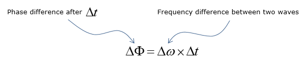
For a constant frequency offset, the phase difference grows linearly with time.
- The equation is ΔΦ = Δω x Δt.
- The label on the left is the phase difference after Δt, and the label on the right is the frequency difference between the two waves.
- The product form holds when Δω stays constant over Δt. Otherwise the integral of the equation above applies.
A number makes this concrete. Let the feedback run 1 kHz above the reference, so Δω = 2π x 1000 rad/s. After 10 microseconds the phase difference is 0.063 rad, or 3.6 deg. After 1 ms it is a full 2π, one complete cycle. So the phase detector sees a phase error that never stops growing, and the loop keeps moving the VCO until the growth stops.
This also gives the meaning of lock. Locked does not mean zero phase difference. It means a constant phase difference, because a constant ΔΦ requires Δω = 0. So when the phase difference stays still, the two frequencies are exactly equal. An XOR loop stays locked with about 90 deg between its inputs, and a PFD loop with close to 0 deg. Both give exactly N x fref at the output.
Phase is the integral of frequency : any frequency offset makes the phase error grow without limit.Lock means a constant phase difference : a phase difference that does not change requires the two frequencies to be equal.A phase detector also detects frequency over time : a 1 kHz offset already moves the phase by one full cycle every 1 ms.