Simply put, RF Transciever IC is an package which has the functionality of RF/Analog Transmition path and reciever path. A transceiver IC sits between the antenna side parts and the baseband chip, and its borders are a design choice rather than a fixed rule. Let's first look at the blocks of a complete transmit and receive path. Then we will see what the IC exchanges with the baseband chip, which blocks can move into the IC, and how the IC helps the PA with power consumption and ACLR.
- What does a transmit and receive path contain ?
- What goes in and out of a transceiver IC ?
- Which blocks can be integrated into the IC ?
- How does a transceiver IC save power and improve ACLR ?
What does a transmit and receive path contain ?
Overall illustration of a transmission and reciever path of a communication device is as shown below. Of course, the circuit on real device would be more complicated than this.. and if the mobile device is a mobile phone supporting multiple technology (e.g, CDMA, GSM, WCDMA, LTE), you would have this kind of blocks for each technology. So if you implement all of these technology using discrete component, it would be a huge job and the size of the mobile phone would be like a small laptop PC. In addition, recently with high end mobile devices (e.g, smart phone), these transciever IC start to have many of intelligent technique to reduce energy consumption (e.g, Evelope Tracking, Average Tracking) and to improve ACLR (e.g, Predistortion).
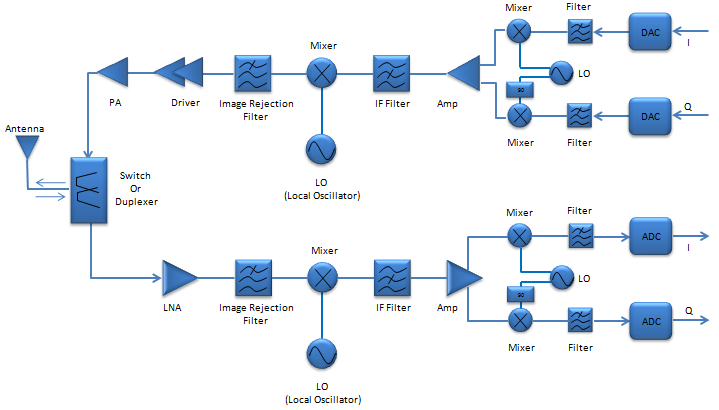
- The transmit path starts at the right. The DACs for I and Q feed filters and two mixers, whose LO is shifted by 90 degrees for the Q branch. The Amp, IF Filter, Mixer, Image Rejection Filter, Driver and PA follow toward the antenna.
- The receive path runs the other way. After the LNA come the Image Rejection Filter, the Mixer, the IF Filter and the Amp, and then the I and Q mixers, filters and ADCs.
- The Switch Or Duplexer connects both paths to one antenna. A TDD system uses a switch, because transmission and reception take turns in time. An FDD system uses a duplexer, because both run at the same time on different frequencies.
The drawing uses two frequency conversions, with an IF stage between them. Many cellular transceivers use a direct conversion design instead. The mixer then converts between RF and I/Q baseband in one step, and the IF Filter, the IF Amp and the second LO disappear. Fewer blocks make integration easier, which is one reason for the popularity of this design. The Homodyne page covers this architecture.
Every supported technology or band adds blocks : a discrete design would need a copy of these paths for each of them.A switch serves TDD and a duplexer serves FDD : the choice depends on whether Tx and Rx share time or share frequency.Direct conversion removes the IF stage : fewer blocks mean a smaller and simpler transceiver IC.
What goes in and out of a transceiver IC ?
The idea on Tranceiver IC is to put all (or most) of these functionality into a single (or only a few) ICs. Very high level view of Transciever IC would be as shown below. On one side, there goes RF input/output and on the other side Analog or Digital I/Q signal comes in and out.
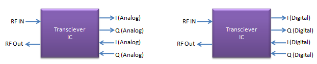
- The left drawing exchanges I (Analog) and Q (Analog) with the baseband side, and the right drawing exchanges I (Digital) and Q (Digital).
- Both drawings have the same RF IN and RF Out on the antenna side.
The choice between the two drawings decides where the data converters sit. With analog I/Q, the ADCs and DACs are in the baseband chip, and analog signals travel across the board between the two chips. These traces pick up noise and crosstalk. With digital I/Q, the transceiver IC contains the converters, and only digital samples leave it. The price is a fast digital interface.
Let's estimate how fast. An LTE carrier of 20 MHz uses a sample rate of 30.72 Msps. Suppose each I and each Q sample has 12 bits. Then one receive chain produces 30.72 x 106 x 2 x 12 = 737 Mbps. A UE with four receive antennas needs about 2.95 Gbps for one carrier, and carrier aggregation multiplies this again. This is why the digital interface between transceiver and baseband is a serial link with its own specification, and not a simple parallel bus.
Analog I/Q leaves the converters in the baseband chip : analog traces between the chips are then sensitive to noise.Digital I/Q moves the converters into the transceiver IC : the interface must then carry hundreds of Mbps per receive chain.
Which blocks can be integrated into the IC ?
Now we would come across a practical questions. What kind of functional blocks (components) should be packed into the IC. The ideal one (what everyone wish to have) would be as the one marked in green line (labeled as (A)). This has everything in it and you only need to hook up an antenna to the chip and you will get baseband digital I/Qs. But at least as of now, this is too good to be true. The second choice would be the one surrounded by the blue line (B). However, even this is very hard to achieve. For some components, it is very difficult to implemement on IC. For example, the final stage power amplifier would be difficult to packed into an IC because it would tend to generate a lot of heat. Oscillators like VCXO,TCXO is also difficult to sit in the IC and some of the filter (e.g, SAW, BAW filter) is also hard to be replaced by silicon technology. As result, a practical transciever IC would be the one surrounded by black line (C) which contains most of function within the IC but some of functions is still implemented as discrete component. Of course, there are a lot of other possibilities of packaging these components into ICs. You may see some other solutions splitting these into multiple ICs as well.
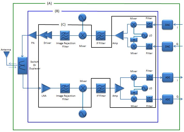
- The green line (A) encloses every block, including the DACs, the ADCs and the Switch Or Duplexer. Only the antenna stays outside.
- The blue line (B) leaves out the Switch Or Duplexer and the data converters. It still contains the PA and the Driver.
- The black line (C) also leaves out the PA, the two IF Filters and the two RF LOs, drawn as the circles above and below the mixers. It keeps the Driver, the LNA, the mixers and the I/Q section.
One of the most common/high end RF Transciever being used in mobile device would be Qualcomm RTR, WTR series.
Why do these blocks stay outside? The reasons are physical, not only a matter of process technology. The PA must deliver about 23 dBm at the antenna connector, and more at its own output. The heat and the supply current of that stage do not fit well on the same die as a sensitive LNA. SAW and BAW filters are acoustic resonators on piezoelectric material, so a silicon process cannot build them. A reference oscillator such as a TCXO needs a quartz crystal for its frequency accuracy and temperature stability. The duplexer is also an acoustic filter, and it carries the full Tx power.
Option A is the goal and option C is the practice : the PA, the acoustic filters and the crystal stay outside the IC.Acoustic filters need piezoelectric material : SAW and BAW filters cannot move into a silicon IC.The PA stays separate for power and heat : it usually goes into the front end module instead, see RF Front End.
How does a transceiver IC save power and improve ACLR ?
The first section mentions Envelope Tracking, Average Tracking and Predistortion. All three help the external PA, but the transceiver IC computes them, because it holds the digital I/Q samples. Let's see what problem each one solves.
The problem starts with PA efficiency. An ideal class B amplifier reaches an efficiency of π/4, or 78.5 %, only when its output swings across the full supply voltage. The efficiency falls in proportion to the output amplitude. At 6 dB below full swing the amplitude is half, so the efficiency is also half, about 39 %. A modulated signal spends most of its time well below its peaks, so a PA with a fixed supply voltage wastes much of its DC power.
Average Power Tracking, usually called APT, lowers the supply voltage when the average output power is low, for example when the UE is close to the base station. The voltage changes only when the power setting changes. Envelope Tracking goes one step further. The supply follows the instantaneous envelope of the signal, so the PA stays close to full swing all the time. The transceiver IC provides the envelope signal, because it knows the I/Q samples before the PA sees them. See Envelope Tracking for details.
Predistortion solves a different problem. A PA driven close to compression distorts the signal, and the distortion spreads power into the adjacent channel. That power appears as poor ACLR. Digital predistortion applies the inverse of the PA nonlinearity to the I/Q samples before transmission, so the PA output is close to linear again. The PA can then run closer to compression, where it is more efficient, while the ACLR still meets the limit.
A fixed supply wastes power at back off : ideal class B efficiency falls from 78.5 % at full swing to about 39 % at 6 dB back off.APT follows the average power, and ET follows the envelope : both reduce the supply voltage when the PA does not need it.Predistortion trades linearity work for efficiency : the IC corrects the PA distortion, so the PA can run closer to compression with acceptable ACLR.