Bias T (Bias Tee) is a special device (3 port device) that is mainly used when we trying to applying some DC power (we call this DC a Bias) to protect the RF component from being damaged by the DC bias.
Many RF parts need a DC supply. An LNA, a transistor amplifier or an active antenna has to be biased, but the RF path must not carry that DC back into the signal source. A Bias T solves both problems with only two components. This page first explains how those two components split DC from RF, and then shows how the device is connected in practice.
How does a Bias T separate DC from RF ?
The whole trick of a Bias T is that a capacitor and an inductor react to frequency in opposite ways. So let's look at each component on its own first, and then check with real numbers how well the pair separates the two paths.
General circuit of a bias T would look as follows. You see the circuit is 'T' shaped and that's why it is called Bias T.
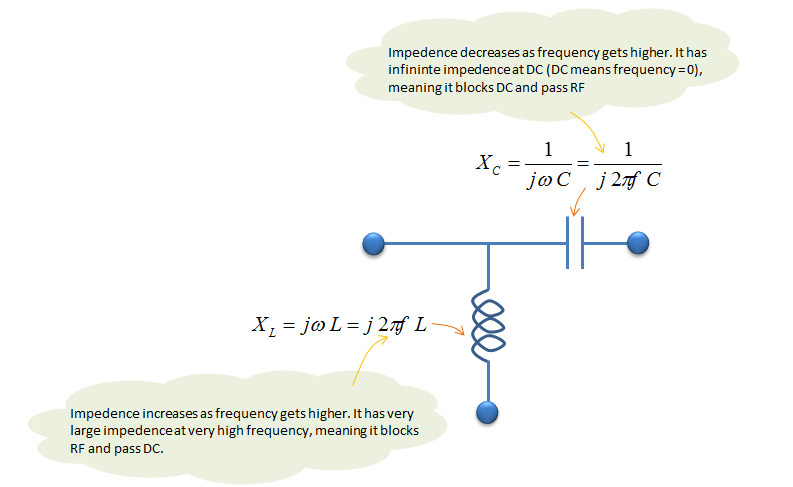
The basic Bias T circuit. The series capacitor passes RF and blocks DC, and the shunt inductor passes DC and blocks RF.
- The horizontal line runs between two ports. A capacitor sits in series on the right part of this line.
- An inductor hangs down from the junction of the T to the third port at the bottom.
- The upper note gives XC = 1/(jωC) = 1/(j2πfC). The impedance falls as the frequency rises and is infinite at DC, so the capacitor blocks DC and passes RF.
- The lower note gives XL = jωL = j2πfL. The impedance rises with frequency and is very large at high frequency, so the inductor blocks RF and passes DC.
The words very large and very small only mean something against the system impedance, which is usually 50 ohm. The capacitor should look much smaller than 50 ohm at the lowest RF frequency, and the inductor should look much larger than 50 ohm. The table below takes C = 100 pF and L = 1 microhenry as an example. The loss and the return loss were computed for ideal components between two 50 ohm ports, with the DC port grounded for RF.
Frequency | |XC| for 100 pF | |XL| for 1 microhenry | RF loss | Return loss |
10 MHz | 159 ohm | 63 ohm | 6.05 dB | 1.2 dB |
100 MHz | 15.9 ohm | 628 ohm | 0.06 dB | 18.5 dB |
1 GHz | 1.59 ohm | 6283 ohm | 0.001 dB | 38.5 dB |
At 10 MHz the pair fails. The capacitor is larger than 50 ohm and the inductor is close to it, so the Bias T loses 6 dB and reflects most of the power. At 100 MHz and above the RF path is almost lossless. So every Bias T has a lowest usable frequency, and larger L and C values move it down. You can estimate the edge of each part on its own. The series capacitor between two 50 ohm ports has a corner at 1/(2π x 100 ohm x C), which is 15.9 MHz here. The shunt inductor sees 25 ohm, the two ports in parallel, so its corner is 25/(2πL), which is 4.0 MHz here.
The highest usable frequency comes from the parts themselves. A real inductor has capacitance between its turns, so above its self resonant frequency it behaves like a capacitor and no longer blocks RF. A real capacitor has lead inductance with the same effect in reverse. So a wideband Bias T often uses several inductors in series, each one covering part of the band.
The two components split the paths by frequency : the series capacitor blocks DC and passes RF, and the shunt inductor passes DC and blocks RF.Very large and very small are judged against 50 ohm : XC must be much smaller and XL much larger than the system impedance at the lowest RF frequency.Every Bias T has a usable band : the L and C values set the lowest frequency, and the self resonance of the real parts sets the highest.
How is a Bias T connected in a real setup ?
A common usage of Bias T is to connect it with RF source and DC power as illustrated below. In this configuration, RF input can be protected from DC source by the mechanism illustrated below. I hope this illustration itself would explain clearly enough.
The picture below adds the three port names to the same circuit. The coloured arrows show where each kind of signal can go, and the red crosses mark where it is stopped.
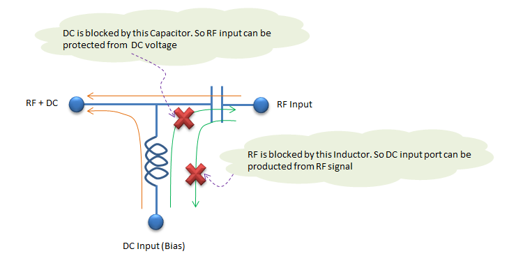
A Bias T in use. RF and DC enter at different ports, leave together at the RF + DC port, and neither one reaches the other source.
- The three ports are RF Input on the right, DC Input (Bias) at the bottom and RF + DC on the left.
- The upper note says the capacitor blocks DC, so the RF input is protected from the DC voltage. A red cross marks this point next to the capacitor.
- The lower note says the inductor blocks RF, so the DC input port is protected from the RF signal. The note spells this word as producted. A second red cross marks this point on the inductor path.
- The orange arrow runs from the DC input up through the inductor and out at RF + DC. The grey arrow along the top runs from the RF input out at RF + DC.
- The green arrows show the two blocked paths: DC towards the RF input, and RF down towards the DC input.
The RF + DC port goes to the part that needs the bias. One common case is a GPS antenna with a built in LNA. The receiver sends DC up the same coaxial cable that brings the RF signal down, so the antenna needs no separate power cable. A tower mounted amplifier at a base station is powered in the same way. On the bench, a Bias T also feeds the drain or collector supply of a transistor amplifier under test.
Two warnings come with this setup. First, the RF + DC port carries the DC voltage. If you connect it to a signal analyzer or a signal generator by mistake, the DC can damage the instrument input. So check the DC input limit of the instrument before you connect it. Second, the inductor carries the full bias current. If the current is above the rating of the inductor, its core saturates, its inductance drops, and it stops blocking RF.
Each port has one job : the RF port carries only RF, the DC port carries only DC, and the RF + DC port carries both to the device.One cable carries both signal and power : this is how an active GPS antenna or a tower mounted amplifier is powered.Check the ratings before you connect : the RF + DC port can damage an instrument input, and too much DC current saturates the inductor.