Impedance was one of very confusing concept (terminology) to me. Followings are the many questions that comes up in my mind when I was first learning the concept of impedance. Are same questions annoying you as well ?
When I first learn about 'Resistance' in high school physics, it said " Resistance is a tendancy to make current flow difficult" and it has sound intuitive to me for long time.
As usual, I just tried to convert into a plain language when I first heard of 'impedance'. But as soon as I tried to convert it into plain language, all the confusion start poping up and I would get more questions as I was trying to get deeper into the concept.
I don't see much difference in terms of plain language between 'Resistance' and 'Impedance'. But if there is no difference, why we need a new terminology ? So... I would say "Resistance" and "Impendance" has very close relationship but not exactly same. Then what is the difference ? This is what I am going to talk in next section.
The picture below collects those questions in one place. Each bubble is answered by one of the sections listed after it. Let's go through them in order, because each answer uses the one before it.
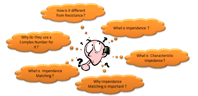
Figure 1. The questions this page answers. They run from the definition of impedance to characteristic impedance and impedance matching.
- What is impedance ?
- Details of Each Impendence Component
- Why we use a complex number for it ?
- What is characteristic impedance ?
- What is impedance matching ?
- How do you measure how well a load is matched ?
- Recommended Video
What is impedance ?
Now let's try to define 'Impdeance' in more formal way. If I am asked to define 'Impedence' in my own words, I would define "Impedance is any form of tendancy to CHANGE the current flow". I used the word 'CHANGE' in my definition, not "OPPOSE" or "MAKE DIFFICULT". Of course, "OPPOSE" or "MAKE DIFFICULT" can be a kind of "CHANGE" but does not explain all aspect of "CHANGE".
I understand you wouldn't much about the math -:), but sometimes it would be clearer/easier to understand a concept if the math is not too complicated. Let's try anyway. You will see the detailed meaning of this formula in following sections. Just try to get the big picture here. Also think about how you would answer the questions I put here.
The diagram below splits the impedance Z into two parts. The resistive component R does not depend on frequency. The reactive component does, and it is the sum of an inductive term jωL and a capacitive term -j/(ωC). The two small graphs at the bottom show how the size of each term changes with ω = 2πf.
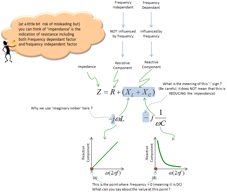
Figure 2. Impedance as a frequency independent part plus a frequency dependent part. The inductive reactance grows with frequency, and the capacitive reactance falls with frequency.
At the point (A) where the frequency is 0, you see the value of Reactive Component is Zero (0). It mean that the reactive factor caused by an Inductor at frequency 0 becomes 0. Meaning the Inductor does not contribute anything to Impendence in DC circuit (you can say 'Frequency = 0' mean DC). Also you can say "L act like 'short' (or just a simple wire) in DC circuit".
At the point (B) where the frequency is 0, you see the value of Reactive Component is Infinity. It mean that the reactive factor caused by a Capacitor at frequency 0 becomes Infinitely large. you can say "C act like 'open' (or just a broken wire) in DC circuit".
Let's put numbers on the two graphs. Take L = 10 nH and C = 1 pF. At 1 GHz the inductor gives ωL = 62.8 ohm, and the capacitor gives 1/(ωC) = 159.2 ohm. At 1 MHz the inductor gives only 0.063 ohm, while the capacitor gives 159 kohm. So at low frequency the inductor is close to a wire, and the capacitor is close to an open circuit. This is exactly what points (A) and (B) say.
Figure 2 also asks what the '-' sign in front of j/(ωC) means. The sign does not make the impedance smaller in size. It tells you that the capacitive term points the opposite way on the imaginary axis from the inductive term. So the two reactances cancel each other when they are equal in size. For the L and C above, this happens at f = 1/(2π√(LC)) = 1.59 GHz, where both reactances are 100 ohm. We call this frequency the series resonance.
Impedance has a frequency independent part and a frequency dependent part : R stays the same at every frequency, while the reactance of L and C changes with f.An inductor is a short at DC and a capacitor is an open at DC : ωL goes to 0 and 1/(ωC) goes to infinity as f goes to 0.The minus sign is a direction, not a reduction : inductive and capacitive reactance point opposite ways, so they cancel at resonance.
Details of Each Impendence Component
Let's look into following three illustration. We have three cases labeled (A), (B), (C) and each of the cases has single component labeled 'R', 'X', 'Y' respectively. Let's assume that we applied the same electrical source suppyplying AC voltage/current. (I will talk later about why I use AC (not DC) source here). On right side, you see the voltage and current graph measured across each of the component.
Do each of the component appose current flow ?
Yes.
How do you know ?
If it does not oppose current flow at all, the current flow should be infinately large.. but they are not infinately large here.. so we can say all of these component oppose(hinder) current flow.
Then what is the difference among the case (A), (B), (C) ?
The difference lies in the phase difference in current curve. In case (A), there is no phase difference between current and voltage curve. But in case (B), there is 90 degree phase difference between the voltage curve and current curve. (In (B), current curve is lagging the voltage curve by 90 degree. In (C), current curve is leading the voltage curve by 90 degree).
The property (tendancy) to change the current flow as in case (A) is called 'Resistance' and The property (tendancy) to change the current flow as in case (B) or (C) is called 'Reactance'.
The electrical device called 'Resistor' has property as in case (A). The electrical device called 'Inductor' has property as in case (B) and the electrical device called 'Capacitor' has property as in case (C).
In the diagram below, blue is the voltage and red is the current in every case. Compare where the red peak sits relative to the blue peak, because that shift is the whole difference between the three cases.
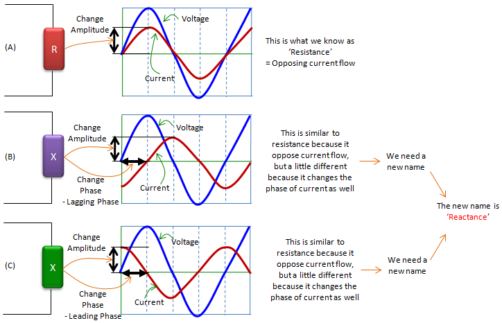
Figure 3. Resistance changes only the amplitude of the current. Reactance changes both the amplitude and the phase, so it needs a name of its own.
Case (A) is a resistor : the current peak and the voltage peak line up, so there is no phase shift.Case (B) is an inductor : the current peak comes a quarter period after the voltage peak. The picture labels this "Lagging Phase".Case (C) is a capacitor : the current peak comes a quarter period before the voltage peak. The picture labels this "Leading Phase".
In real circuit (especially in AC circuit), there is not so many cases where you use only single type of component like type (A), (B), or (C). In most case, a circuit is made up of the combination of all of these types.
And in reality, there is no devices which shows 100% of type (A) property and 0 % of type (B)/(C), and there is no device which shows 100% of type (B)/(C) property and 0 % of type (A). I would say every electrical device has at least a little bit of all of these three properties in it. So if we take a look at the current flow of overal circuit (or a block of circuit), we would see the combined effect of all the type (A), (B), (C). This combined property of type (A), (B), (C) is called 'Impedance' as illustrated below. As you see in this illustration, the impedance indicates two properties of current flow changes (current opposition property and phase change property) simultaneously.
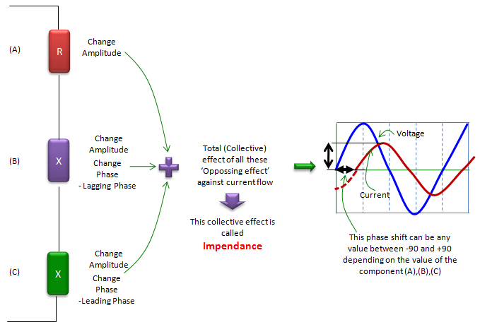
Figure 4. Impedance is the combined effect of R, L and C. The phase shift of the current can be any value between -90 and +90 deg, depending on the values of the components.
The phase shift in Figure 4 has a simple formula. For a series circuit with resistance R and net reactance X, the voltage leads the current by the angle θ = arctan(X/R). A positive X, which is inductive, gives a positive θ, so the current lags. A negative X, which is capacitive, gives a negative θ, so the current leads. The angle reaches +/-90 deg only when R is 0, which is the pure reactance of cases (B) and (C).
Every real part is a mix of R, L and C : a resistor has lead inductance, and an inductor has winding resistance and capacitance between turns.The sign of the net reactance decides lag or lead : an inductive circuit makes the current lag, and a capacitive circuit makes it lead.
Why we use a complex number for it ?
As I mentioned above, 'Impedence' is an indicator to show the combined properties of 'Resistance' and 'Reactance'. Then how can we represent this multiple properties in mathematical terms. You can think of a couple of possibility. One possibility is just to represent it as two separate numbers. Another possibility is to represent it in a vector with two element, and another possibility is to represent it as a complex number.
What would be the best option ? It would be hard to mathematically prove which one is the best choice but it is most widely accepted to represent it as a complex number. The relationship between Registance/Reactance and the real/imaginary part of complex number is illustrated as below.
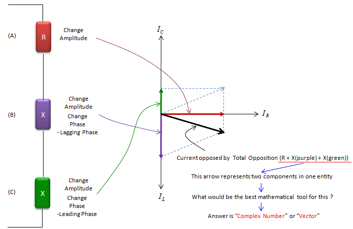
Figure 5. The total opposition to current has two components, so it is one arrow in a plane. A complex number or a two element vector can carry both components.
If you plug each electrical component (R,L,C) into the case shown above, you would understand how these electrical component properties can be represented in the complex number of Impedance. See the illustration below.
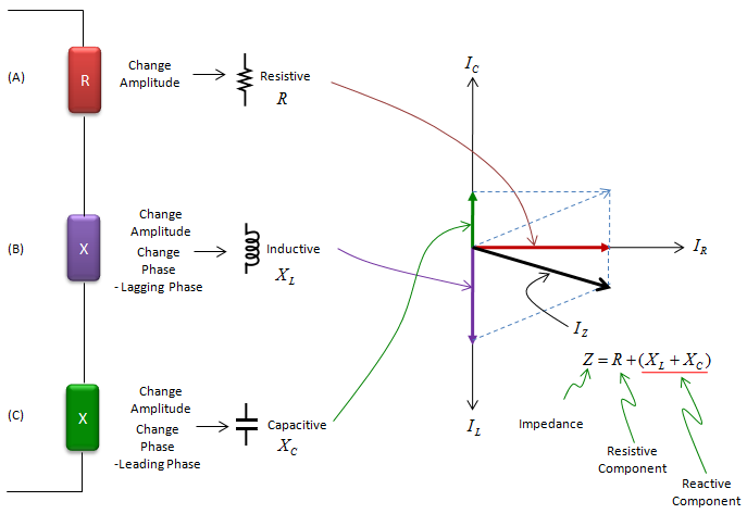
Figure 6. The resistor maps to the real part of Z, and the inductor and the capacitor map to the imaginary part.
Figures 5 and 6 label the axes with currents: IR to the right, IC up and IL down. This is the current phasor picture, where a capacitor current leads and an inductor current lags. When you draw the impedance itself, the axes are R and X instead. Then the inductive reactance points up, the capacitive reactance points down, and the two pictures are mirror images of each other.
Why does a complex number win over a plain two element vector? The reason is that circuit rules need multiplication and division, not only addition. Ohm's law V = I x Z multiplies two complex numbers. The magnitudes multiply, and the phase angles add, so one operation gives both the new amplitude and the new phase. A vector has no such product.
Let's try it on a series R, L, C circuit with R = 50 ohm, L = 10 nH and C = 1 pF at 1 GHz. Series impedances add, so Z = 50 + j62.8 - j159.2 = 50 - j96.3 ohm. The magnitude is |Z| = 108.5 ohm, and the angle is -62.6 deg. The negative angle tells you that the circuit is capacitive at this frequency, and the current leads the voltage by 62.6 deg.
Real part is resistance, imaginary part is reactance : Z = R + jX, with X = ωL - 1/(ωC) for a series circuit.Complex arithmetic handles amplitude and phase together : series impedances add, and V = I x Z multiplies magnitudes and adds phases.The angle of Z is the phase between voltage and current : in the example, -62.6 deg means a capacitive circuit with a leading current.
What is characteristic impedance ?
Figure 1 asks one question that the sections above have not answered yet. What is characteristic impedance, and why is it 50 ohm on almost every RF cable? The answer matters because the matching sections below compare every load against it.
At RF, a cable or a PCB trace is often longer than a small part of a wavelength. So the signal travels along it as a wave. In a wave that travels in one direction, the ratio of voltage to current is fixed by the line itself. This ratio is the characteristic impedance Z0. It depends on the geometry and the dielectric of the line, and it does not depend on the length of the line.
For a lossless line, Z0 = √(L/C), where L and C are the inductance and the capacitance per unit length. For a coaxial cable this becomes Z0 = (60/√εr) x ln(D/d). Here D is the inner diameter of the outer conductor, d is the diameter of the centre conductor, and εr is the relative permittivity of the dielectric. With polyethylene, εr = 2.25, and a ratio D/d = 3.5 gives 50.1 ohm. For 75 ohm with the same dielectric, D/d has to be 6.52.
So why 50 ohm? For an air-filled coax, the loss from conductor resistance is lowest near 77 ohm. The peak power before voltage breakdown is highest at 30 ohm. 50 ohm sits between these two optimums. Many RF systems therefore use it as a common reference, and 75 ohm is common where low loss matters most, such as video and cable TV.
Z0 belongs to the line, not to the load : it is the voltage to current ratio of a wave travelling in one direction.Geometry and dielectric set Z0 : for coax, 60/√εr x ln(D/d). Length does not change it.50 ohm is a compromise : it sits between the 77 ohm lowest loss point and the 30 ohm highest power point of an air coax.More detail : see Characteristic Impedance and Coax.
What is impedance matching ?
In most electrical circuit or a system, Energy is supplied from a source and go through multiple intermediate blocks and finally reaches the output of the circuit/system. And we usually tries to convey the energy from to source to the output with as little loss as possible. To minimize the energy loss while the energy propagate from one block to another block, one of the most important condition is that the impedance of a block and the impedance of next block should be same. Impedance Matching is a process (practice) of making the impendance of neighbouring blocks 'Matched'. (I used the term 'Matched', not 'Same'. You will see why later).
Impedance matching is one of the most important things in most RF circuit design and implementation. It normally requires not only some theory behind it but also a lot of experience.
Even more tricky thing is that a condition for impendance matching at a specific frequency may not work at another frequency. So it tends to be very difficult to find the best impedance matching condition for a component which has to work in wide frequency range (e.g, Wide band RF filters).
Putting it into an illustration, it can go as follows.
If you put some energy into a component (labeled as (A)) and transfer it to a next block (labeled as (B)), the energy may split into three portions. Some portions would get transferred to (B) as we want, but some portion would bounce back to (A) and some other portion would get lost (dissipate as heat).
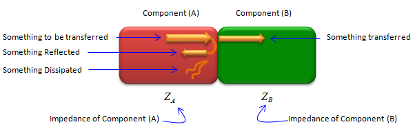
Figure 7. At the boundary between two blocks, the energy splits into a transferred part, a reflected part and a dissipated part. ZA and ZB decide the split.
Our goal here is to maximize the portions of energy being transferred and minimize the engergy that is bounced back or lost. One way to do that is to adjust the impedance of each block so that they become 'matched'.

Figure 8. Impedance matching adjusts ZA and ZB so that the transferred part is as large as possible.
Then what does it mean by 'Matched' ? i.e, what is the condition for 'Matched Impedance' ? The answer can be summarized as below.
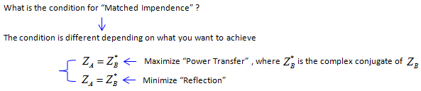
Figure 9. Two matching conditions for two goals. The conjugate match maximizes power transfer, and the equal impedance match minimizes reflection.
Be careful with the second line of Figure 9. It writes ZA = ZB* for both goals, but the condition for minimum reflection is ZA = ZB, without the conjugate. On a transmission line, the reflection coefficient at the load is Γ = (ZL - Z0)/(ZL + Z0), and it is 0 only when ZL = Z0. This is why the page says 'Matched' rather than 'Same'. When both impedances are real, such as 50 ohm and 50 ohm, the two conditions give the same answer.
Let's see the conjugate match with numbers. Take a source of 1 V rms with an internal impedance ZS = 25 + j10 ohm. The power into a load is |V|2 x RL/|ZS + ZL|2. With ZL = 25 - j10 ohm, the reactances cancel, and the load receives 10 mW. With ZL = 25 + j10 ohm, which is equal to ZS rather than its conjugate, the load receives only 8.62 mW. A plain 50 ohm load receives 8.73 mW.
Maximum power transfer needs the conjugate : ZL = ZS* cancels the reactance of the source.Zero reflection on a line needs ZL = Z0 : this is the condition behind a VSWR of 1.A match holds only over a band : reactance changes with frequency, so a network matched at one frequency is usually not matched at another.
How do you measure how well a load is matched ?
A perfect match is rare, so engineers need a number that says how far a load is from it. Four numbers are in common use, and they all come from the same reflection coefficient Γ. The table below gives them for a few loads on a 50 ohm line.
Load ZL |
|Γ| |
VSWR |
Return loss |
Mismatch loss |
50 ohm |
0 |
1.0 |
infinite |
0 dB |
75 ohm |
0.2 |
1.5 |
14.0 dB |
0.18 dB |
100 ohm or 25 ohm |
0.333 |
2.0 |
9.5 dB |
0.51 dB |
The formulas are short. VSWR = (1 + |Γ|)/(1 - |Γ|). Return loss = -20 log10|Γ| in dB, so a larger return loss means a better match. Mismatch loss = -10 log10(1 - |Γ|2) in dB, and it is the part of the power that never enters the load. Notice that 100 ohm and 25 ohm give the same |Γ|. Only the sign of Γ differs, so the four numbers alone cannot tell you whether a load is too high or too low.
The mismatch loss is often smaller than people expect. A VSWR of 1.5 costs only 0.18 dB of power. Even so, the reflected wave can still matter, because it can disturb a power amplifier or create ripple in a filter response.
One Γ, four views : VSWR, return loss and mismatch loss are all functions of |Γ|.Higher return loss is better : 14 dB return loss corresponds to a VSWR of 1.5.More detail : see Reflection Coefficient, VSWR and Return Loss.
Recommended Video
The two videos below are a two part tutorial on electrical impedance. They are useful as a second explanation of the ideas in the first three sections of this page.