Microstrip and stripline are the two transmission line structures you meet most often on an RF circuit board. Both are a flat conductor trace over a ground plane, with a dielectric substrate between them. They differ in where the trace sits, and that single difference changes the speed, the loss and the isolation of the line. This page starts with the two structures and then shows how the dimensions of a microstrip set its characteristic impedance.
- What is a Microstrip ?
- How is a Stripline different ?
- What do you decide before the design ?
- How do the dimensions set the impedance ?
What is a Microstrip ?
Let's start with the cross section, because every property of the line follows from it. The drawing below shows three layers: a trace on top, a dielectric substrate in the middle and a ground plane at the bottom.
Microstrip is a electronic structure in which a transmission line(conductive trace line) sitting on top of a dielectric material which is in between the transmission line and ground plane as illustrated below.
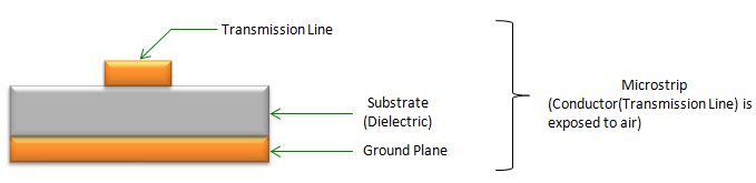
Microstrip cross section. The trace is exposed to air on its upper side.
Notice the note on the right of the drawing: the conductor is exposed to air. So the electric field of the line runs partly through the substrate and partly through the air above it. The wave therefore sees an effective dielectric constant εeff between 1 and εr. For the same reason a microstrip line is called quasi-TEM rather than TEM. It can also radiate, which is useful for a patch antenna and unwanted for a filter.
In this aspect, almost any trace line you see in most electric circuit board can be called a Microstrip. But we don't call any trace line on the circuit board as a microstrip. Normally when we call it as microstrip, normally those structure is intentionally designed to perform a special functions like filters or antenna etc. Some of the examples of Microstrip are shown below.

Microstrip used as a circuit element. The shape of the trace, not a discrete component, sets the function.
- Example (a) is a test board with a meandering trace between two coaxial connectors.
- Example (b) is part of a product board, with two microstrip structures marked by red frames.
- Example (c) is an array of repeated microstrip elements on a gold-plated substrate.
A microstrip is a trace over a ground plane : the dielectric substrate sits between the trace and the ground.The field runs in two media : part of it is in the substrate and part in the air, so εeff lies between 1 and εr.The trace shape is the component : filters, couplers and antennas are drawn directly in copper.
How is a Stripline different ?
A stripline moves the trace inside the board. That one change removes the air from the field, and the rest of this section follows from it.
Very similar to microstrip, there is another structure called Stripline. The key difference between Microstrip and strip line is the location of transmission line. In microstrip, the transmission line is sitting on top of dielectric material whereas in stripline the transmission line is embedded in the dielectric material and ground planes are on both sides of the transmission line as shown below.
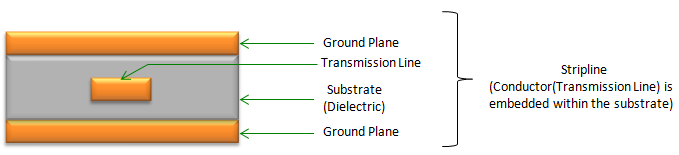
Stripline cross section. The trace is embedded in the substrate between two ground planes.
Because the whole field sits inside a uniform dielectric, a stripline carries a true TEM wave, and its effective dielectric constant equals εr. The wave is therefore slower than on a microstrip over the same substrate. For example, with εr = 4.4 a wavelength at 2.4 GHz is 124.9 mm in free space and 59.6 mm in the stripline. The two ground planes also shield the trace. So a stripline radiates very little and couples less to its neighbours. The price is access. You cannot place a component on a buried trace, and every connection to the surface needs a via.
The whole field is in the dielectric : a stripline is a TEM line with εeff = εr.Two ground planes give shielding : a stripline radiates less and couples less to other traces than a microstrip.A buried trace needs vias : components mount on the surface, so a microstrip is easier to tune and to probe.
What do you decide before the design ?
As the operation speed (e.g, clock speed) of an electric system or frequency of wireless communication system goes higher the importance of microstrip and stripline gets higher, When we try designing microstrip or stripline, you need to have clear answers to some of basic questions as illustrated below.
The picture below collects those questions around a thinking figure. Each question fixes one input of the calculation in the next section.

Questions to answer before a microstrip or stripline design. The answers become the target impedance, the dimensions and the substrate.
- The upper left cloud asks for the function. The examples given are filter, antenna and coupler.
- The upper right cloud asks for the characteristic impedance to meet. This is the target Zo, usually 50 ohm.
- The lower left cloud asks how big and how thick the device should be. This limits H, W and the length of the line.
- The lower right cloud asks which substrate material can be used. This fixes εr and the loss tangent.
The substrate question matters twice. Its εr sets the impedance and the wavelength, and its loss tangent sets the dielectric loss of the line. The Loss Tangent page shows how to turn the loss tangent into dB.
The function comes first : a filter, an antenna and a coupler need different trace shapes and different tolerances.The target impedance is an input : the dimensions are chosen to meet it, not the other way round.The substrate fixes two numbers : εr for impedance and wavelength, and the loss tangent for loss.
How do the dimensions set the impedance ?
Once you determined answers to the questions regarding the design goal, you have to determine the basic electrical properties of the microstrip and stripline. Most important electric properties of the structure would be Characteristic impedence and capacitance. These electrical properties are determined mainly by the dimmension of the microstrip/stripline and the dielectric material as examplified below. The equation shown here may be a little different from what you see from other source. Just try to understand a general tendancy from these equation. In practice these days nobody is designing microstrip/stripline using these simple equation. In most case they use very expensive softwares (HFSS, Microwave Studio, Maxwell etc) to calculate these electric properties by directly solving maxwell equations.
The drawing below names the four inputs. W is the width of the trace, T is its thickness, H is the height of the substrate and εr is its dielectric constant. The two formulas under it give the characteristic impedance Zo in ohm and the capacitance Co in pF per inch.
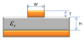
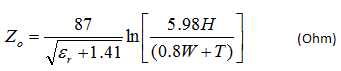
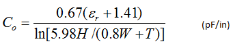
Microstrip dimensions and the simple formulas for Zo and Co. Only ratios of lengths enter the formulas, so any length unit works.
- Zo = 87 / √(εr + 1.41) x ln[5.98 H / (0.8 W + T)], in ohm.
- Co = 0.67 (εr + 1.41) / ln[5.98 H / (0.8 W + T)], in pF/in.
Some of the general tendancy you can directly read from these equation shown above are
- As the thickness of dielectric substrate (separation between transmission line and ground plane) gets larger, characteristic impedence of the structure gets larger.
- As the dielectric constant of the dielectric substrate gets larger, characteristic impedence of the structure gets smaller.
- As the width of the transmission line gets larger, characteristic impedence of the structure gets smaller.
- As the thickness of the transmission line gets larger, characteristic impedence of the structure gets smaller
Let's put numbers into the Zo formula. Take a substrate with εr = 4.4, a typical value for FR-4, with H = 1.6 mm and T = 0.035 mm. A 50 ohm line then needs W = 2.95 mm. From that starting point, the formula shows each tendency above. Doubling H to 3.2 mm raises Zo to 75 ohm. Lowering εr to 3.0 raises it to 57 ohm. Doubling W to 5.9 mm lowers it to 25 ohm.
How far can you trust the simple formula? One check is to compare it with the more accurate closed-form Hammerstad formulas used in most microwave textbooks. On this substrate the two agree within 1.5 ohm for W/H between 0.3 and 1.9. They drift apart for wider traces. At W/H = 2.5 the simple formula gives 39.1 ohm and the Hammerstad formula gives 42.5 ohm. For the 50 ohm line above the Hammerstad formula asks for W = 3.08 mm instead of 2.95 mm.
The same model also gives εeff. For the 50 ohm line it is about 3.33, between 1 for air and 4.4 for the substrate. So a wavelength at 2.4 GHz is 68.4 mm on this line, and a quarter-wave section is 17.1 mm long. That length is the one a microstrip filter or matching stub is built from.
Zo depends on ratios of dimensions : scaling W, T and H together leaves the impedance unchanged.A 50 ohm line on 1.6 mm FR-4 is about 3 mm wide : 2.95 mm by the simple formula and 3.08 mm by the Hammerstad formula.The simple formula is good for narrow traces : it drifts from the more accurate model once W/H goes above about 2.The line length depends on εeff : at 2.4 GHz a quarter wavelength on this line is 17.1 mm, against 31.2 mm in air.