Digital Transciever Interface
This topic will deal with the issues of how to send a digital data from one point to another point. I will be mostly focus on high data rate technology. So I would not talk much of the common technology you might have heard so often like old type PC Serial Port or Printer port. The purpose of this page is to give you a brief introduction on high speed digital transciever technologies that is becoming more and more of hot topics recently.
Probably this device (or communication method) has been the major issue since the first invention of any kinds of digital devices (including computer and almost all the wireline digital communication).
Brief history of the evolution of the Digital Transciever
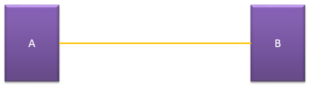
As you can easily guess (or might have experienced by yourself), the first type of digital transciever technology is based on Serial communication as illustrated below. Logically it is just a single electrical line between one point to another point. (In reality, even the serial communication is not a single line. It usually is made up of multiple lines e.g, Tx and Rx lines and ground and some additiona protocol line. However, if you focus only on data line regardless of direction, you can simplify this as a single line as follows)
So far so good. Simple concept and simple design. Then what would be the problem ? Why we needed any further evolution ?
It is because of the same reason as in any kind of communication. On day 1, they invent a technology for a certain type of communication and on Day 2 and forever they keep thinking of how to increase the data rate, i.e, how to increase the speed of the communication.

How to increase the data rate ? The first thing you can think of would be just to increase the clock rate of the transmitter and reciever. It is pretty sure that this kind of effort was made at early stage. But the technology at the early stage was not good enough to achieve the enough data rate just by increasing the clock speed.
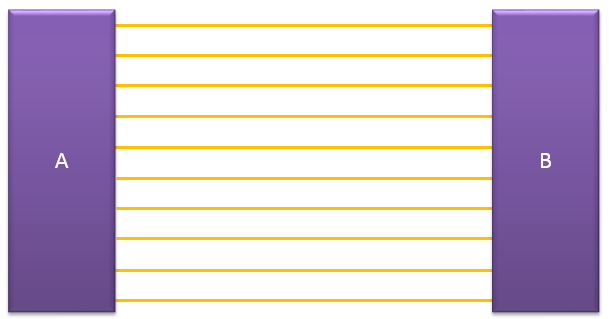
What would be the next option ? The next option is to transmit the data in multiple parallel lines as shown below. It is like increasing the amount of traffic of cars by widening/adding more lanes on highway. Also, there was another motivation going forward to parallel lines. Most of the diginal processors exchanges data with outside world using multiple parallel I/O pins. So it would be easier to implement the interface between the core chipset and external interface.
Now you have a new technology implemented. What would be the next question ? Yes, you're right. The same question : How to increase the data rate ?
Theoretically there are more options to increase the data rate comparing to the case of serial communication. The first option would be to increase the number of lines and the second option would be to increase the clock rate. To a certain degree, any of these options would work and there had been evolutions with these options.
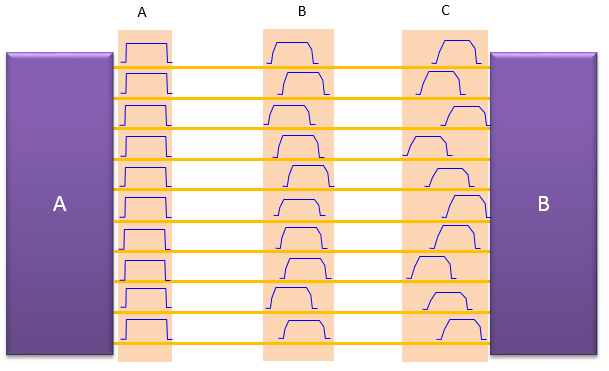
However, you cannot increase the data rate infinately with these methods. First, can we increase the number of data lines infinately ? Definately the answer is No because we don't have infinate space in any hardware to put the infinate number of data lines. Then, can we increase the clock rate infinately ? You know the answer is No. Comparing to serial communication, there is another problem with the increased clock rate. It is the timing skew issue. By the law of physics, the signal gets destorted and speed of the electric signal varies as it travel along the signal line as illustrated below. At the starting point of the transmitted signal shown at column (A), the signals on all the data line is not distorted and well aligned in time, but as it travel down the signal path, the signal start getting distorted in amplitude and dispersed in timing as you see in column (B). By the time the signal reaches the reciever, the distortion and time dispersion would get so bad that it would cause a lot of decoding errors.
At the end of the eveolution of the parallel communication, we have a question of how to remove the timing skew and as energy efficiency of the system gets more and more important we get to have another question 'how to drive this communication system at a very low energy concumption ?' meaning 'How to maintain the reliable decoding at very low driving voltage ?'

Do we have any answer to these questions ? Yes, we have. Ironically, the answer is 'Going back to our old friend ; Serial Communication'. Then you may ask 'How the old fashioned serial communication can solve these problems ?'. Actually, it is not only the serial method itself that solves these problem. There has been drastic improvement in semiconductor technology to help the solution working.
It would be obvious (easy to understand) on how serial communication can solve the timing skew issue. Of course, there still be a certain degree of time dispersion (delay spread) on serial data line, but at least you don't have to worry about the synchronizing these dispersed signal among multiple data lines.
Also there has been another very important evolution in the area of semiconductor. The transistor switching speed has become lightening fast and the driving voltage drop has continually evolved.
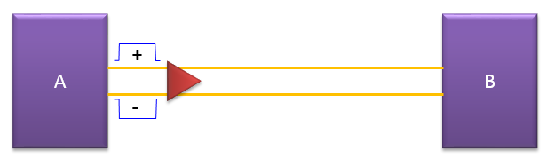
Another important invention that has helped the improvement is Balanced signal (Balanced Circuit) as illustrated below. This helps the serial communication not only in terms of lowering driving voltage but also in terms of the resistance to noise.
With this invention, we would have the same question again. How to increate the data rate ?
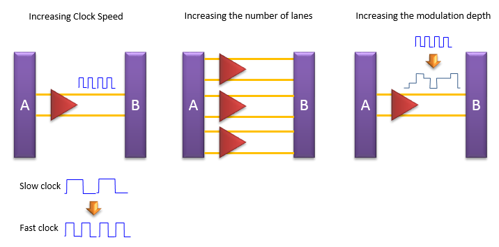
The most common methods that are employed are roughly three types as illustrated below. The first method is obvious. Just to increase the clock rate. The second method is also what anybody can guess. It is to increase the number of lanes. This is not the parallel communication. It is multiple separate serial communication. The third one would not be what many of digital people would have thought, but it is one of the most common techniques to be used to increase the data rate in Analog or RF communication. It is to apply high depth modulation scheme like PAM4, PAM8 or 16 QAM etc.
Since the rebirth of the serial communication, we have seen ever evolving serial communication method for the past decades and this evolution continues even now .. and now (as of 2015) we are talking about 400 Gb communication.
(I will write further on these new evolution later in this page or post a new page). In this evolution, these three methods are employed in various combinations, meaning in some case only one specific method (e.g, increasing clock rate only or increasing the number of lanes only) and in some other case two or more methods are applied in combination. Followings are some of the examples of this evolution.
|
Data Rate/Application |
Clock |
Number of Lanes |
Modulation |
|
10 Ghz |
1 |
|
|
|
10 Ghz (10.3125 G) |
4 |
|
|
|
10 Ghz (10.3125 G) |
10 |
|
|
|
400 Gb Ethernet |
25 Ghz |
16 |
NRZ |
|
25 Ghz |
4 |
PSM4 |
|
|
50 Ghz |
4 |
PAM4 |
Technology components of Digital Transciever
In some sense, what I have described above is just with an aspect of a concept, it is not about real hardware. When it comes to implementing those concepts, it would boil down to an electronic device or circuit. In this section, I will describe on various type of electronic device or circuit that are used to implement the technologies described above.
Most of the conetents of this page is based on an Whitepaper from Altera (Ref [1]). I will add additional contents as I learn more.
TTL(Transistor to Transistor Logic) :
- The most common and basic of I/O standards.
- Operates with a +5V power supply
- Transmit at speeds up to 100 MHz.
- TTL tends to require high quiescent current particularly in the faster device families (Disadvantage).
- Suffer in certain implementations because device transistors are required to be either saturated or completely off. This requirement causes switching to be slow because the load capacitances take time to either fully charge or discharge.
Low Voltage TTL (LVTTL) :
- Invented to improve the drawback of TTL and improve the performance
- Operate at reduced power consumption by reducing the voltage swing required to change state
- Support higher data rates
ECL(Emitter Coupled Logic)/CML(Current Mode Logic) :
- Used as an alternative to traditional TTL logic because it is better suited for highspeed data transmission.
- Operate in the active region and therefore do not suffer from the same transistor switching issues found in TTL.
- A small DC bias is placed on the base of the transistor, resulting in a small voltage swing from base to emitter, and allowing the device to change state more quickly.
- Relies on the emitter current flow for operation rather than the precise voltage levels used in TTL, causing a greater current draw. As a result ECL is also known as Current Mode Logic (CML) due to the high amounts of current flowing through the transistors.
- Widely used in sections of telecommunications equipment applications, generating logicfamilies such as the 1000H and 10000H.
- ECL requiresrelatively high current (Drawback).
- Relies on a negative power supply for operation (Drawback). This can cause problems when interfacing to positive-supply-based devices residing in the rest of the system.
PECL(Positive Emitter Coupled Logic) :
- Invented to overcome the drawback of PCL (relying on negative power supply and causing issues with interfacing with positive-voltage-based logic families such as TTL and CMOS)
- Has similar performance properties to ECL but operates from a positive voltage rail making it simpler to integrate into a digital system.
- Still suffers from the power issues as ECL
LVDS(Low Voltage Differential Signaling) :
- Based on CMOS logic
- Perform at high speed with low noise generation, EMI resistance, and low power requirements.
- Used in high bandwidth data transfer applications, in particular backplane transceivers or clock distribution applications.
- Operate at low signal swing voltage of 350 mV, much lower than TTL, ECL and CMOS. This lower swing voltage presents added benefits over other alternatives as follows
- Power efficient. AC power is low because the signal switch-over voltage is small, leading to low power dissipation per signal transition. DC power is also low because although each channel requires 3.5 mA, it is likely a single channel will be replacing a number of existing parallel channels.
- Generates reduced levels of EMI. Device-generated EMI is dependent on frequency, output voltage swing and slew rate. Due to the low-voltage swing of the LVDS standard, the effects of EMI are much less than with CMOS, TTL, or other I/O standards.
- Defined by two similar industry standards supporting different data rates:
- IEEE 1596.3 supports data rates up to 250 Mbps
- ANSI/TIA/EIA-644 recommends a higher data rate of up to 655 Mbps. This standard suggests a theoretical maximum of 1.923 Gbps (based on a lossless medium) and provides recommendations for fail-safe operation for the receiver under fault conditions.
LVPECL(Low Voltage Positive Emitter Coupled Logic) :
- Low voltage differential version of PECL, commonly used in video graphics, data communication and telecommunication applications.
- Forms the signaling standard for a number of protocols including Gigabit Ethernet and Fibre Channel.
- Similar to LVDS, but operates with a larger differential voltage swing.
- Tends to be a little less power efficient than LVDS due to its ECL basis, however it can operate at frequencies above 1 Gbps due to its high speed switching characteristics.
PCML(Pseudo Current Mode Logic) :
- High speed differential architecture derived from CML logic and is capable of speeds in excess of 2 Gbps.
- Operates at a 3.3-V power supply (at 1.5 V in later specification), higher than LVDS and LVPECL, but uses a lower swing voltage, allowing for faster switching.
- Better power characteristics than its ECL ancestors, but has higher power consumption than other differential I/O standards not based on the current mode configuration.
- Widely adopted for use at data rates of 2.5 Gbps and above.
- Used in a variety of applications including networking and data communications.
HyperTransport Technology I/O :
- Formerly known as Lightning Data Transport (LDT)
- Developed to support next generation chip to chip interfaces for computer based equipment.
- Used as the signaling interface for the HyperTransport protocol ( HyperTransport has been developed as an enhanced version of LVDS, employing a larger voltage swing).
- Requires a 100 Ω differential terminator at the receiver buffer which make it a more robust interface when used in an application with relaxed Printed Circuit Board (PCB) layout requirements.
PCI Express (also known as 3GIO and Arapahoe) :
- Developed to provide a high speed backplane alternative to PCI.
- Makes use of high speed transceiver technology to overcome the speed and layout limitations of the original PCI specification.
Reference :
[1] The Evolution of High-Speed Transceiver Technology - Whitepaper, Altera
[2] Multi-Gigabit SerDes: The Cornerstone of High Speed Serial Interconnects