Permittivity is very vague concept.. very hard to grasp the meaning at least to me. But It is very important concept because a lot of other important concepts are derived from this concept.
If you google the meaning of Permittivity, the most common definition would be as follows : Permittivity (Absolute Permittivity) is the measure of the resistance that is encountered when forming an electric field in a medium.
Does this make any sense to you ? At least not much to me.
So this page builds the meaning from pictures instead. It starts with what an electric field does to the charges in a dielectric, and then connects permittivity to electric flux density and to capacitance. After that it shows what permittivity changes for an RF signal, and it closes with a table of typical values.
- Polarization and Permittivity
- Electric Flux Density and Permittivity
- Permittivity and Capacitance
- Permittivity at RF
- Permttivity Table
Polarization and Permittivity
Let's start inside the material. A dielectric has no free electrons, so an electric field cannot drive a current through it. What the field can do is pull the charges inside each molecule a little apart, and permittivity describes how far they move for a given field.
Whenever you have a difficult concept, one big help would be to come up with an example (real or imaginary). Let's make an imaginary examples as shown below.
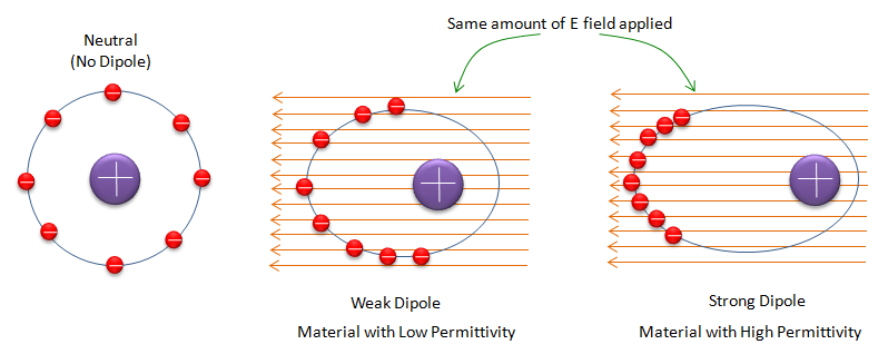
The first one (the left one) shows a molecule and it's charge distribution when there is no electric field applied (Don't try argue with illustration of exact charge distribution .. quantom physics .. I know it is not very accurate illustration). In the first illustration, you see the negative charges are relatively evenly distributed around the positive charge. You can take this first picture as a reference state to compare with other cases (second and third one).
Now let's suppose that electric field is applied through the molecules of two different material (the second and third one).
From the common sense from high school physics, you would guess that negative charges and positive charges would move in opposite directions. (Note : we assume that this materials are dielectric materials and the charges moves but within a certain boundary. In case of conductor, the negative charges (free electrons) gets out of the molecule flows towards the one end).
Due to this movement in opposite direction, you would see the separation (polarization) of charges. But if you compare the second and third one, you see stronger separation in the third one than in the second one. The stronger separation you see, you would say it has higher permittivity.
Following is the mathematical expression that explain the exact thing that I mentioned above.
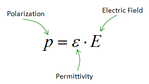
Now just "READ" or "Verbalize" the equation above and you would get the intuitive meaning of it.
- Degree of polarization is directly proportional to the electric field applied.
- The stronger the applied electric field, the stronger polarization it shows.
- Permittivity is the proportional coefficient linking Polarization to the applied Electric Field.
- 'Strong Permittivity' means you can achieve the same degree of polarization with less Electric Field.
The equation above keeps the picture simple, and it is worth knowing the exact form behind it. In a linear material the polarization is P = ε0 χ E, where χ is the electric susceptibility. The permittivity is ε = ε0 (1 + χ). So the precise coefficient between P and E is ε - ε0, not ε itself. The difference is ε0, the part of the permittivity that exists even in vacuum, where nothing can polarize. The intuitive reading of the bullets still holds, because a larger χ gives both a stronger polarization and a larger ε.
Engineers rarely quote ε in F/m. They quote the relative permittivity εr = ε / ε0 = 1 + χ, which is a plain number. Vacuum has εr = 1, and air is very close to 1. Every other material has εr greater than 1, because its charges can be polarized.
An E field separates the charges of a dielectric into dipoles : the charges move but stay bound to their molecules.High permittivity means strong polarization for the same field : the right hand molecule in the illustration of three molecules shows this case.The exact relation is P = ε0 χ E : the coefficient is ε - ε0, and the relative permittivity is εr = 1 + χ.
Electric Flux Density and Permittivity
Polarization describes the material. For circuit and field calculations we need a quantity that combines the applied field and the response of the material. That quantity is the electric flux density D, and permittivity links it to E in one exact equation.
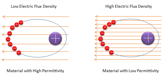
Let me give you another set of illustrations which has same meaning described above but with a little bit different perspective. If you see the first and the second illustration, you would see the same degree of separation of electric charges (separation of positive and negative charges). Then what is difference ?
In the first illustration, you would see less number of electric field lines than in the second one. It means that less amount of electric field can produce the same degree of polarization.
Again, if I express the illustration into a mathematical form, it is as follows.
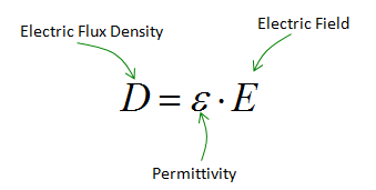
Now just "READ" or "Verbalize" the equation above and you would get the intuitive meaning of it.
- Electric Flux Density is directly proportional to the electric field applied.
- The stronger the applied electric field, the higher Electric Flux Density it gets.
- Permittivity is the proportional coefficient linking Electric Flux Density to the applied Electric Field.
- 'Strong Permittivity' means you can achieve the same Electric Flux Density with less Electric Field.
The two equations on this page fit together through one more relation, D = ε0 E + P. The first term is the flux the field would create in vacuum, and the second term is the contribution of the polarized material. Putting P = ε0 χ E into it gives D = ε0 (1 + χ) E = ε E, which is the equation above.
This relation also explains the titles in the pair of illustrations above. Both molecules show the same charge separation, so P is the same in both. The low permittivity material needs more field lines, a larger E, to reach that P. Its ε0 E term is therefore larger, and so its D is higher. That is why the right hand picture carries the title High Electric Flux Density.
D matters in practice because it is set by the free charge. Gauss's law says that the flux of D out of a closed surface equals the free charge inside it. So a charge placed on a conductor fixes D, and the material then decides E through E = D / ε. A material with higher permittivity carries the same charge with a weaker field and, as the next section shows, with a lower voltage.
D = ε E is exact for a linear material : it follows from D = ε0 E + P with P = ε0 χ E.D is fixed by the free charge : the permittivity then decides how strong the E field is for that charge.High permittivity gives a weaker field for the same charge : this is the property that a capacitor uses.
Permittivity and Capacitance
Capacitance is where permittivity turns from a field property into a circuit value. Two conductors separated by a dielectric store charge, and the permittivity of that dielectric decides how much charge they store for each volt. The effect appears whether we build the capacitor on purpose or not.
If you apply a voltage (electric field) on both side of a material, you can create a capacitance. Sometimes you would want to make this kind of capacitor intentionally but sometimes this capacitance would be generated even when you don't want it. Physics doesn't care of your intention, the law applies the same if all the conditions are same.
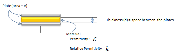
The Capacitance build up by the structure illustrated above can be calculated as follows. (From this formula, you would notice the higher permittiviy, the larger capacitance you will get)
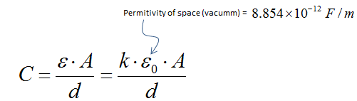
- The drawing labels the relative permittivity as k. It is the same quantity as εr in the previous sections, and the formula writes ε = k ε0.
- The note above the formula gives the permittivity of vacuum, ε0 = 8.854 x 10⁻¹² F/m.
- The formula assumes that the plates are large compared with d, so the field is uniform between them and the fringing field at the edges can be ignored.
Let's put numbers into the formula. Take two copper areas of 1 cm2 on the two sides of a 1.6 mm FR4 board, with k = 4.7. Then C = 4.7 x 8.854 x 10-12 x 10-4 / (1.6 x 10⁻³), which is about 2.6 pF. At 1 GHz this capacitance has a reactance of about 61 ohm. That is close to the 50 ohm of a typical RF line, so a copper area of this size is not a small detail at RF. It is a real part of the circuit, even when nobody drew it on the schematic.
Capacitance grows in direct proportion to permittivity : doubling k doubles C for the same plates and spacing.C = k ε0 A / d : larger plates and a thinner dielectric also give more capacitance.Unwanted capacitance matters at RF : 1 cm2 of copper over 1.6 mm FR4 is about 2.6 pF, or about 61 ohm at 1 GHz.
Permittivity at RF
At RF the permittivity of the material around a conductor does more than set a capacitance. It changes the speed of the wave, its wavelength and the impedance it sees. So the choice of board material sets the physical size of every RF structure on it.
A wave in a medium with relative permittivity εr travels at v = c / sqrt(εr), assuming a non magnetic material. The wavelength shrinks by the same factor, λ = λ0 / sqrt(εr). The wave impedance of the medium also falls, from about 377 ohm in free space to 377 / sqrt(εr) ohm. The table below shows these values for a 3.5 GHz wave, whose free space wavelength is 8.57 cm.
Material | εr | v / c | λ at 3.5 GHz | Wave impedance |
Teflon | 2.1 | 0.69 | 5.91 cm | 260 ohm |
Oxide | 3.9 | 0.51 | 4.34 cm | 191 ohm |
FR4 | 4.7 | 0.46 | 3.95 cm | 174 ohm |
Silicon | 11.68 | 0.29 | 2.51 cm | 110 ohm |
These values hold for a wave that travels completely inside the material. A microstrip line is different, because part of its field runs in the air above the board. So the line sees an effective permittivity between 1 and εr, and its wavelength lies between the two limits. A quarter wave stub on FR4 is therefore shorter than in air, but not by the full factor of the table.
Permittivity is also not a single real number at RF. It is written as a complex value, ε = ε' - j ε''. The real part ε' is the permittivity discussed so far. The imaginary part ε'' describes energy lost as heat when the dipoles follow the alternating field. The ratio ε'' / ε' is the loss tangent, tan δ. Both parts change with frequency, so a datasheet value for εr is always given at a stated frequency.
Higher permittivity slows the wave : v = c / sqrt(εr), so on FR4 the wave travels at about 0.46 c.Wavelength shrinks by the same factor : RF structures on a high permittivity substrate are smaller than in air.A microstrip sees an effective permittivity : its value lies between 1 and the εr of the board.At RF permittivity is complex and frequency dependent : the imaginary part sets the dielectric loss through tan δ.
Permttivity Table
The table below lists typical relative permittivity values. Treat them as a starting point, not as design values. The permittivity of a real material depends on its exact composition, on the frequency and on the temperature, so an RF design takes εr from the datasheet of the actual material. In the table, Oxide means silicon dioxide, the insulating layer in silicon chips.
|
Material |
Relative Permittivity |
|
Air |
1 |
|
Glass (standard) |
7.6~8.0 |
|
Plexiglass |
~2.8 |
|
Rubber |
2~7 |
|
ABS (Plastic) |
2.0~3.5 |
|
Teflon(PTFE : Polytetrafluoroethylene) |
2.1 |
|
Mica |
3~6 |
|
Paper |
3.85 |
|
FR4 |
4.7 |
|
Oxide |
3.9 |
|
Diamond |
5.5-10 |
|
Silicon |
11.68 |
Let's read the table by groups. Air sits at 1, the lower limit for any material. The plastics, Teflon, ABS and Plexiglass, sit between 2 and 3.5. Teflon is the base of many low loss RF substrates, because its low permittivity keeps the lines wide and its loss is small. FR4 is the common board material for digital and low cost RF circuits, and its value depends on the mix of glass and resin in a given laminate. Silicon has the highest value in the table, so structures on a silicon chip see a wavelength less than a third of the free space value.
Where a row gives a range, such as Rubber or Mica, the material comes in many compositions. Pick the datasheet of the grade you actually use, and check the frequency at which the value was measured.
The table gives typical relative permittivity values : a design uses the datasheet value of the actual material at the working frequency.Low permittivity plastics suit RF substrates and covers : Teflon at 2.1 changes the wave the least of the solid materials listed.Silicon at 11.68 shortens the wavelength the most : the wave on a silicon chip travels at about 0.29 c.