What is RF Front End (RFFE) ? As for many other technical terms, the term "RF Front End" has several different variations of definitions from narrow to wide meaning. I would introduce two different versions of definition that I think defines well. I strongly recommend you to read the both references that I linked here and it will give you pretty good big picture on RF Front End.
Let's start with the two definitions and see where each one draws the border. Then we will look at why the front end moved into integrated modules, how those modules connect to the baseband chip, and why the number of parts grows so quickly with MIMO and bands. The last section puts numbers on the price of that growth: every switch and filter adds loss, and the loss costs transmit power and receive noise figure.
- How is the RF Front End defined ?
- RF Front End Getting Into a Chip and Why ?
- Several different implementations of RF Front End
- Complexity Explosion ?
- Any Idea to prevent the complexity explosion ?
- How much do the front end losses cost the Tx and Rx paths ?
- Reference
How is the RF Front End defined ?
The border of the front end is not a physical line on the board. Different documents draw it at different places, so the same word can refer to a small module or to almost the whole radio. Before reading any datasheet or market report, we should know which border it uses.
According to Reference [1], RF Front End is defined as follows :
The RF front end is generally defined as everything between the antenna and the digital baseband system. For a receiver, this "between" area includes all the filters, low-noise amplifiers (LNAs), and down-conversion mixer(s) needed to process the modulated signals received at the antenna into signals suitable for input into the baseband analog-to-digital converter (ADC). For this reason, the RF front end is often called the analog-to-digital or RF-to-baseband portion of a receiver.
According to this definition, roughly the area in the gray area would be defined as RF Front End.
[Figure 1]
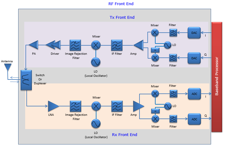
- The Tx path runs from right to left. The two DACs produce the I and Q signals, and the two mixers with the LO and the 90 degree block combine them. The chain then continues through Amp, IF Filter, a second Mixer, Image Rejection Filter, Driver and PA.
- The Rx path runs from left to right. It goes through the LNA, Image Rejection Filter, Mixer, IF Filter and Amp, and then splits into the I and Q mixers, filters and ADCs.
- Both paths meet at the Switch Or Duplexer, which connects them to one antenna. Everything except the Baseband Processor sits inside the gray RF Front End box.
- The drawing shows a two step conversion with an IF stage. A direct conversion receiver removes the IF stage and mixes straight to I and Q, as explained in Homodyne. The border of the definition stays at the data converters either way.
According to Reference [4], it is stated as follows.
The RFFE in a UE is made up of a number of key components:
- The antenna(s) and antenna tuner(s)
- Band Select, Duplexers: filters, duplexers, diplexers, and switches used for frequency control
- Transmitters and RF Power Amplifiers (Tx/PA’s)
- Receivers and Low-Noise Amplifiers (Rx/LNAs)
The Baseband and RF (mixers, down converter, etc.) section, a key component in the overall UE, is not part of the RFFE
According to this definition, the RF Front End can be highlighted in gray as follows :
[Figure 2]
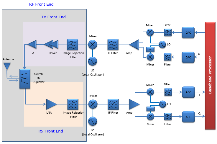
- The gray box now covers only the Switch Or Duplexer, the PA and Driver, the LNA and the two Image Rejection Filters.
- The mixers, the LOs, the IF filters and the data converters sit outside the box, next to the Baseband Processor.
Which one is the correct definition ? Both can be correct depending on the context. I personally use the first definition when I am referring to RFFE(RF Front End) in this page. However, most of the detailed description would be around the section in the second definition.
The second definition also matches the way the parts are sold. One chip, usually called the RF transceiver, holds the mixers, the LOs and the data converters. The PAs, LNAs, switches and filters come as separate front end modules, often from other vendors. So when a market report counts front end content in a phone, it normally means the parts inside the gray box of Figure 2.
The wide definition ends at the data converters : it includes every analog stage between the antenna and the ADC or DAC.The narrow definition ends at the PA and the LNA : it includes the antenna side parts only and leaves the mixers and converters to the transceiver.Check the definition before comparing numbers : the size, cost and loss of the front end change a lot with the border.
RF Front End Getting Into a Chip and Why ?
In recent radio technology, at least speaking of cellular phone, the area for PCB(Printed Cirbuit Board) is not so wide in a mobile phone as highlighted in red shown below. Even in the limited area, the space that can be allocated for RF front end is only a small portion of the PCB. It is very difficult (almost impossible) to put all of the discrete RF component in the area.
[Figure 3]
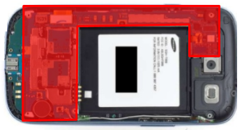
You may say 'recently we see tendancies for the size of the mobile phone to get larger and larger. and we would have larger spaces for RF components'. However, it is only one aspect. As we see larger device in one aspect, we see larger battery size due to higher energy comsumption requirement and there are more requirement for a phone to support more bands (different frequencies) and multi mode(GSM, WCDMA, LTE all in single phone). Therefore, the space for RF front end is still tight.
Even with assumption that you have enough space to put all those components in discrete manner, you would need to invest a lot of time and effort to tune and match each and every discrete components. (Of course, this way of implementation would create a best job market for RF engineers :)
One of the best solution would be to put all of those components into one or a few small packages and use them like an IC (Integrated Circuit). As far as I know as of now (Mar 2018), almost every cellular device use this kind of integrated RF IC (module) rather than using discrete devices.
If you are more interested in what kind of RF Front End module are used in real commercial phone, see Ref[8] which would show you very nicely summarized examples from various commercialized phone.
There is also a performance reason for integration. Every connection between two discrete parts needs a matching network, and every matching network has its own loss and its own tolerance. Inside a module, the vendor designs and tests these connections once. The phone maker then sees only the ports of the module, specified at 50 ohm, and the tuning work moves from each phone design to the module design.
PCB area is the first reason for integration : the space left for the front end is small, and the number of bands keeps growing.Tuning effort is the second reason : a module arrives already matched, so the phone design does not need to tune each discrete part.
Several different implementations of RF Front End
Once all (or most) of RF components get into a chip (or package), integrating the RF into a device (e.g, mobile phone) is like a digital embedded system rather than RF/Analog system. Admitting that this might be oversimilification, modern mobile phone structure in terms of radio stack hardware can be illustrated as follow. As you see here, even though most of the discrete RF components are analog devices the front end chipset (or the package) become like a digital chipset. It provides various control and data line that communicate with micro controller chipset(Baseband chip in this case).
[Figure 4]
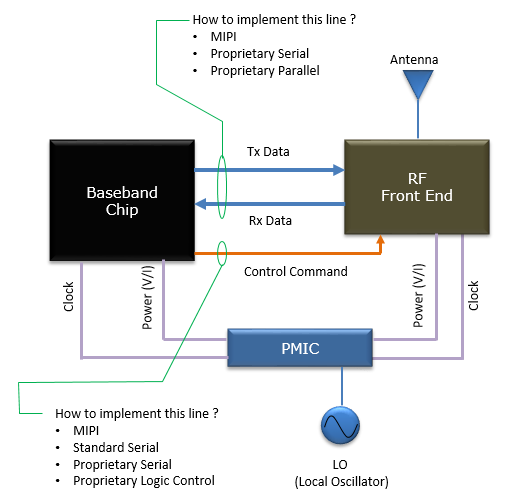
- The blue lines carry Tx Data and Rx Data, and the orange line carries the Control Command from the Baseband Chip to the RF Front End.
- The PMIC supplies Power (V/I) and Clock to both chips, and the LO is drawn under the PMIC.
- The two callouts list the options for each line. For the data lines they are MIPI, Proprietary Serial and Proprietary Parallel. For the control line they are MIPI, Standard Serial, Proprietary Serial and Proprietary Logic Control. MIPI RFFE is the MIPI interface for front end control.
The illustration shown above is the case of maximum integration of RF Front End in which all of the RF components (e.g, PA, LNA, Filters) and Up/Down converters are integrated in a single chip. This might be the best solution for the hardware engineers who has to design and implement the board. However, there are some cases where we implement the RF Front End as two chip as illustrated below. In this type, pure RF components (Amplifier, Switch / Diplexer / Duplexer) are integrated in a separate chipset from the Up/Down Converter chipset. This type of architecture would add a little bit more complexity comparing to the previous architecture, but there is motivation for this type of architecture. It is hard for one company to be the best for every field. There can be a company that is more specialized in Up/Down Converter and DAC/ADC part and another company that is better fit for pure RF modules. By adopting this architecture, we can better optimize the hardware performance. Or in somecases this architecture may save hardware cost as well if you are good enough at bargaining with two different component vendors :).
[Figure 5]
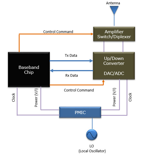
- The Amplifier Switch/Diplexer chip connects to the Antenna, and the Up/Down Converter DAC/ADC chip sits between it and the Baseband Chip.
- Tx Data and Rx Data go only to the converter chip, while Control Command lines go to both chips.
By extending the logic mentioned above to a little bit further, we may think of using Tx RF module (PA module) and Rx RF module (LNA) in seprate chipset as illulstrated below.
[Figure 6]
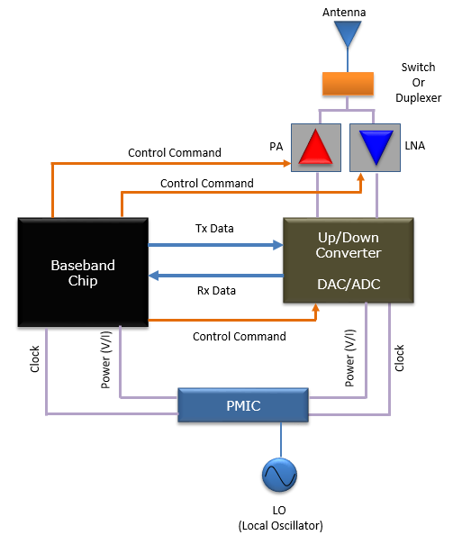
- The PA, drawn in red, and the LNA, drawn in blue, are now separate chips under a common Switch Or Duplexer.
- Each of the PA, the LNA and the Up/Down Converter receives its own Control Command line from the Baseband Chip.
- More separate parts mean more control lines and more RF connections to route on the board. The integration of Figure 4 trades this routing for a single, more complex chip.
Complexity Explosion ?
You may easily guess the functionality of the modern mobile phone has become extremely complicated in terms of radio stack. The driving force for these complexity can be listed as below (as of Mar 2018) :
- Multi-Mode : Single UE supports multiple Radio Technologies like GSM/GPRS, UMTS(WCDMA,TDSCDMA), LTE and 5G/NR in near future
- More (Higher) MIMO : 2x2, 4x4 and even 8x2 Downlink MIMO and possibily more MIMO in 5G/NR.
- More CA(Carrier Aggregation) : 2CC, 3CC, 4CC, 5CC CA in LTE and 16 CC CA in 5G/NR specification.
- More Bands : around 10 different bands in WCDMA and several dozen / ever increasing number of Bands in LTE and additional bands in GSM/GPRS.
How these complexity of the radio stack impact on the complexity of RF Front End structure ? Speaking of the complexity, we may think of complexity in Up/Down converter and ADC, and pure RF part (PA, LNA, Filter Switch). Even though the radio stack complexity would lead to complexity of both part, the impact will be bigger on pure RF part. So let's think of the impact on the complexity of pure RF part here.
First, let's think of the case where we add more MIMO/Diversity functionality and guess how the RF part gets complicated. Intuitively you can think of a progression as illustrated below.
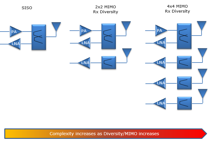
- SISO needs one PA, one LNA, one duplexer and one antenna.
- 2x2 MIMO Rx Diversity adds one receive branch: an LNA, a receive filter and a second antenna.
- 4x4 MIMO Rx Diversity adds three receive branches. The transmit side still has one PA, because the progression here is for downlink MIMO.
Now think of the case where we add more radio technology or bands and see how this influence on the RF part complexity. This progression can be illustrated as follows.
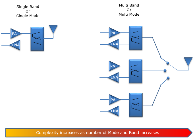
- Each additional band or mode needs its own PA, LNA and duplexer, because a duplexer passes only the band it is designed for.
- A switch selects one of the three duplexers and connects it to the single antenna. This switch is a new part that the single band case does not need, and it adds loss to both the Tx path and the Rx path.
Now a question would pop up in your mind ? What if we add both more MIMO and more bands simultaneosuly ? You can guess easily that I am running out paper to plot multiple cases here for comparision -:), so I would show only one case as below.
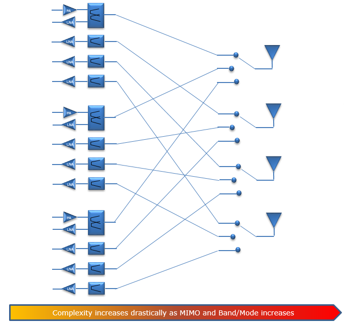
- The drawing shows three bands with 4x4 receive MIMO. Each band has one PA and LNA pair on a duplexer and three extra receive branches, so there are twelve receive branches in total.
- Four antennas each carry a switch with three positions, one for each band. The crossing lines show the routing problem that appears on the board.
- The number of receive branches is the number of bands times the number of receive antennas. So the part count grows as a product, not as a sum.
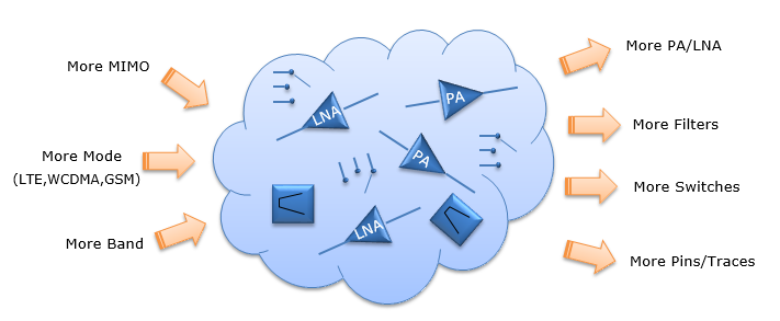
Summing up all of what is mentioned above, we can reach a simple / illustrative conclusion as shown below in terms of the complexity of RF Front End and the factors that lead to the complexity.
Then another question would arise in your mind ? Would this complexity would hit any maximum point and we cannot add any more function ?
If you just think of putting the components in linear fashion as illustrated above, you may reach the point where you cannot add any more parts in small front end chipset. However we have always seen such a great minds that overcome almost every hurdles in engineering. It applies to this area as well. RF frontend manufactureres have made a lot of efforts to optimize and simplify the front end design even with more functionality. One example is show below. This is from Reference [7]. This shows an example of integrating the PAs, switches and filters into three front-end modules that cover the low (a) mid (b) and high (c) bands. Considering the number of bands it supports, you would see that is is simpler than you might have imagined.
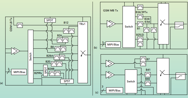
- Module (a) covers the low bands. It holds the GSM LB Tx path, the duplexers for B12, B26, B8, B28A, B20 and B28B, a receive filter for B29Rx, several switches and the TRx1 antenna switch.
- Module (b) covers the mid bands: GSM MB Tx, B34/39Tx, B34/4/66, B1 and B25.
- Module (c) covers the high bands. B7 uses a duplexer, while B41 and B40 use single filters, because B40 and B41 are TDD bands and do not need to separate Tx from Rx in frequency.
- B29 appears as receive only, because it is a downlink only band, 717 MHz to 728 MHz in 36.101 Table 5.5-1.
- Each module has one MIPI/Bias block with three lines. The baseband chip sets the band, the switch positions and the PA mode through this control interface.
MIMO multiplies the receive branches : every extra receive antenna needs its own LNA, filter and switch path in every band.Bands multiply the filters : an FDD band needs its own duplexer, and a TDD band needs its own filter.Integration groups the bands by frequency range : low, mid and high band modules keep the part count on the board small.
Any Idea to prevent the complexity explosion ?
As mentioned above, there has been a lot of effort to reduce the complexity as we put more functionalities into a Front End module. What kind of idea is out there to achieve this goal ? Several ideas are known as below. Some of them are already being used and some of them are at the stage of investigation.
- Tunable matching circuit for Antenna : By using the tunable matching circuit, we may reduce the number of antenna and switches.
- Multi-mode Amplifier and Amplifier Sharing : By using those amplifiers that can support multi-mode (i.e, multiple radio technologies like GSM, WCDMA, LTE) and by sharing an amplifier for multiple bands / modes, we can reduce the complexity of the front end.
- Tunable Filters : As of now (Mar 2018), this still remain as a 'wish list', not an achieved goal. There has been several ideas on tunable filters but not yet meeting the performance criteria of SAW / BAW / FBAR filters.
- Advanced Packaging : As technology evolves in each RF components, the size of each discrete components tend to get smaller and smaller, but as we put more and more devices in the chip and we need more spaces for wiring them together. As a result, wiring/bonding spaces are becoming an issue. We are expecting more idea about packaging to come out to minimize these issues.
Let's look at why the first and the third ideas are hard. An antenna tuner changes the matching or the resonance of the antenna with switched or variable capacitors. It lets one antenna cover more bands, but the tuner itself has loss, and the capacitors must survive the full PA voltage. A tunable filter is harder still. SAW and BAW filters get their frequency from the geometry of an acoustic resonator, such as the electrode pitch or the thickness of a piezoelectric layer. These dimensions are fixed at manufacture. A tunable circuit can change its frequency, but so far it has not reached the steep skirts and the low loss of an acoustic filter.
Tuning replaces parallel parts with one adjustable part : an antenna tuner or a shared amplifier covers several bands that would otherwise need separate hardware.Acoustic filters are fixed by their geometry : this is why each band still needs its own SAW or BAW filter.Every adjustable part has a cost in loss : the next section shows what that loss means in transmit power and noise figure.
How much do the front end losses cost the Tx and Rx paths ?
Every switch and filter that the complexity adds sits between the antenna and the PA or LNA. So the front end loss grows with the part count. Let's put numbers on that loss, because it appears twice: once as extra power the PA must produce, and once as extra noise figure in the receiver.
The table below uses an assumed loss for each part between the antenna and the amplifiers. The values are only an example for this calculation. Real values depend on the band, the part and the vendor, so take them from the datasheets of the actual modules.
Part | Assumed loss | In the Tx path | In the Rx path |
Antenna switch | 0.5 dB | yes | yes |
Duplexer | 2.0 dB | yes | yes |
Total between antenna and PA or LNA | 2.5 dB | 2.5 dB | 2.5 dB |
First, the Tx path. The UE maximum output power in 36.101 is defined at the antenna connector, and it is 23 dBm for Power Class 3 in Table 6.2.2-1. With 2.5 dB of loss after the PA, the PA must deliver 25.5 dBm. That is 355 mW instead of 200 mW, so the PA produces 1.8 times the power that reaches the antenna. Suppose the PA converts 40 % of its DC input into RF output. Then it draws about 890 mW from the battery, compared with about 500 mW with no loss after it.
Next, the Rx path. Loss in front of the LNA adds to the noise figure dB for dB. Let's take an LNA with a noise figure of 1.5 dB and a gain of 15 dB, followed by stages with a noise figure of 10 dB. The Friis formula gives 2.3 dB for the LNA and the later stages alone. With the 2.5 dB of switch and duplexer loss in front, the result is 4.8 dB. So the sensitivity becomes 2.5 dB worse, exactly by the loss. The cascade rule is on the Noise Figure page.
This is why the complexity of the previous sections matters beyond the board area. A second switch in series, or a filter that must reject one more nearby band, adds a few tenths of a dB. On both paths, that loss comes straight out of the link budget.
Tx power is specified at the antenna connector : the PA must produce the front end loss on top of 23 dBm for Power Class 3.2.5 dB of loss nearly doubles the PA output power : 25.5 dBm is 355 mW, compared with 200 mW at the antenna.Loss before the LNA adds directly to the noise figure : 2.5 dB of front end loss raises the receiver NF from 2.3 dB to 4.8 dB in the example.
Reference
[1] What's in an RF Front End? (EE Times)
[2] RF front-end solutions for mobile applications (Infineon)
[3] SKY68001-31: LTE Universal Multi-Band Front-End Module for IoT
[4] Wireless Handset RF Front-End Optimization (4G Americas)
[5] SKY66420-11: 860 to 930 MHz RF Front-End Module
[6] Smartphone Hardware Architecture (Slideshare)
[7] Evolution of the Smartphone (Microwave Journal)
[8] In 5G smartphone designs, RF Front-End graduates from traditional supporting role to co-star with modem